
User guide

DS679F1 23
CS42L51
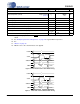
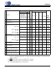
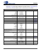
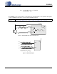
SWITCHING CHARACTERISTICS - SPI
™
CONTROL PORT
(Inputs: Logic 0 = DGND, Logic 1 = VL)
20. Data must be held for sufficient time to bridge the transition time of CCLK.
21. For f
sck
<1 MHz.
Parameter Symbol Min Max Units
CCLK Clock Frequency
f
sck
06.0MHz
RESET Rising Edge to CS Falling
t
srs
20 - ns
CS
Falling to CCLK Edge
t
css
20 - ns
CS
High Time Between Transmissions
t
csh
1.0 - µs
CCLK Low Time
t
scl
66 - ns
CCLK High Time
t
sch
66 - ns
CDIN to CCLK Rising Setup Time
t
dsu
40 - ns
CCLK Rising to DATA Hold Time (Note 20)
t
dh
15 - ns
Rise Time of CCLK and CDIN (Note 21)
t
r2
-100ns
Fall Time of CCLK and CDIN (Note 21)
t
f2
-100ns
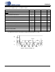
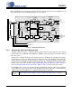
CS
CCLK
CDIN
RST
t
srs
t
scl
t
sch
t
css
t
r2
t
f2
t
csh
t
dsu
t
dh
Figure 7. Control Port Timing - SPI Format