
User guide
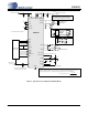

20 DS679F1
CS42L51
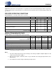
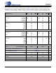
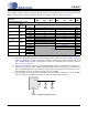
COMBINED DAC INTERPOLATION & ON-CHIP ANALOG FILTER RESPONSE
Notes:
12. Response is clock dependent and will scale with Fs. Note that the response plots (Figure 38 to Figure 41
on page 82) have been normalized to Fs and can be de-normalized by multiplying the X-axis scale by Fs.
13. Measurement Bandwidth is from Stopband to 3 Fs.
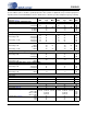
SWITCHING SPECIFICATIONS - SERIAL PORT
(Inputs: Logic 0 = DGND, Logic 1 = VL, SDOUT C
LOAD
= 15 pF.)
Parameter (Note 12) Min Typ Max Unit
Frequency Response 10 Hz to 20 kHz
-0.01 - +0.08 dB
Passband to -0.05 dB corner
to -3 dB corner
0
0
-
-
0.4780
0.4996
Fs
Fs
StopBand
0.5465 - - Fs
StopBand Attenuation (Note 13)
50 - - dB
Group Delay
- 10.4/Fs - s
De-emphasis Error Fs = 32 kHz
Fs = 44.1 kHz
Fs = 48 kHz
-
-
-
-
-
-
+1.5/+0
+0.05/-0.25
-0.2/-0.4
dB
dB
dB
Parameters Symbol Min Max Units
RESET pin Low Pulse Width (Note 14)
1-ms
MCLK Frequency
1.024 38.4 MHz
MCLK Duty Cycle (Note 15)
45 55 %
Slave Mode
Input Sample Rate (LRCK) Quarter-Speed Mode
Half-Speed Mode
Single-Speed Mode
Double-Speed Mode
F
s
F
s
F
s
F
s
4
8
4
50
12.5
25
50
100
kHz
kHz
kHz
kHz
LRCK Duty Cycle
45 55 %
SCLK Frequency
1/t
P
-64•F
s
Hz
SCLK Duty Cycle
45 55 %
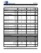
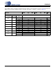
LRCK Setup Time Before SCLK Rising Edge
t
s(LK-SK)
40 - ns
LRCK Edge to SDOUT MSB Output Delay
t
d(MSB)
-52ns
SDOUT Setup Time Before SCLK Rising Edge
t
s(SDO-SK)
20 - ns
SDOUT Hold Time After SCLK Rising Edge
t
h(SK-SDO)
30 - ns
SDIN Setup Time Before SCLK Rising Edge
t
s(SD-SK)
20 - ns
SDIN Hold Time After SCLK Rising Edge
t
h
20 - ns