
User guide
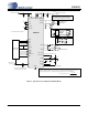

DS679F1 11
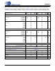
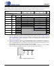
CS42L51
+1.8V or +2.5V
1 µF
VQ
DAC_FILT+
0.1 µF
1 µF
DGND
VL
0.1 µF
+1.8V, 2.5 V
or +3.3V
I²S/LJ
MCLKDIV2
RESET
LRCK
AGND
DEM
MCLK
SCLK
0.1 µF
VA_HP
VD
* Capacitors must be C0G or equivalent
150 pF
AFILTA
AFILTB
150 pF
SDIN
SDOUT/
M/S
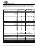
CS42L51
1 µF
**
+1.8V or +2.5V
AOUTB
AOUTA
470Ω
470Ω
C
C
R
ext
R
ext
See Note 2
AIN1A
Left Analog Input 1
1800 pF
1800 pF
100 kΩ
100 kΩ
100 Ω
100 Ω
AIN1B
Right Analog Input 1
*
*
For best response to Fs/2 :
()
4704
470
×
+
=
ext
ext
RFs
R
C
π
This circuitry is intended for applications where the CS42L51 connects directly to an unbalanced output of the device . For
internal routing applications please see the DAC Analog Output Characteristics section for loading limitations .
Note 2 :
Digital Audio
Processor
0.1 µF
VA
Headphone Out
Left & Right
Line Level Out
Left & Right
Speaker Driver
FLYP
FLYN
VSS_HP
GND_HP
10 µF
ADC_FILT+
1 µF
1 µF
51.1 Ω
0.022 µF
VL or DGND (1)
1 µF
See Note 4
Note 4:
Series resistance in the path of the power supplies (typically
used for added filtering) must be avoided. Any voltage drop
on VA_HP will directly impact the negative charge pump
supply (VSS_HP) and result in clipping on the audio output .
1 µF
1 µF
**
**
* *Use low ESR ceramic capacitors.
(1) Pull-up to VL (47 kΩ for Master Mode.
Pull-down to DGND for Slave Mode.
Figure 2. Typical Connection Diagram (Hardware Mode)