CS42L51 Low Power, Stereo CODEC with Headphone Amp DIGITAL to ANALOG FEATURES ANALOG to DIGITAL FEATURES 98 dB Dynamic Range (A-wtd) 98 dB Dynamic Range (A-wtd) -86 dB THD+N -88 dB THD+N Analog Gain Controls – +32 dB or +16 dB MIC Pre-Amplifiers Headphone Amplifier - GND Centered – – – – – On-Chip Charge Pump Provides -VA_HP No DC-Blocking Capacitor Required 46 mW Power Into Stereo 16 Ω @ 1.8 V 88 mW Power Into Stereo 16 Ω @ 2.
CS42L51 SYSTEM FEATURES GENERAL DESCRIPTION 24-bit Converters The CS42L51 is a highly integrated, 24-bit, 96 kHz, low power stereo CODEC. Based on multi-bit, delta-sigma modulation, it allows infinite sample rate adjustment between 4 kHz and 96 kHz. Both the ADC and DAC offer many features suitable for low power, portable system applications. 4 kHz to 96 kHz Sample Rate Multi-bit Delta Sigma Architecture Low Power Operation – Stereo Playback: 12.93 mW @ 1.
CS42L51 TABLE OF CONTENTS 1. PIN DESCRIPTIONS - SOFTWARE (HARDWARE) MODE .................................................................. 7 1.1 Digital I/O Pin Characteristics ........................................................................................................... 9 2. TYPICAL CONNECTION DIAGRAMS ................................................................................................. 10 3. CHARACTERISTIC AND SPECIFICATION TABLES .................................................
CS42L51 4.5.3 High-Impedance Digital Output ............................................................................................. 40 4.5.4 Quarter- and Half-Speed Mode ............................................................................................. 40 4.6 Digital Interface Formats ................................................................................................................ 40 4.7 Initialization ..........................................................................
CS42L51 11. PARAMETER DEFINITIONS .............................................................................................................. 83 12. PACKAGE DIMENSIONS ................................................................................................................. 84 THERMAL CHARACTERISTICS ........................................................................................................ 84 13. ORDERING INFORMATION ...................................................................
CS42L51 LIST OF TABLES Table 1. I/O Power Rails ............................................................................................................................. 9 Table 2. Hardware Mode Feature Summary ............................................................................................. 27 Table 3. MCLK/LRCK Ratios ....................................................................................................................
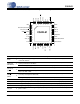
CS42L51 Pin Name # SDIN SCLK MCLK SDOUT (M/S) DGND VD VL RESET 1.
CS42L51 AOUTB AOUTA 10 11 Analog Audio Output (Output) - The full-scale output level is specified in the DAC Analog Characteristics specification table VA 12 Analog Power (Input) - Positive power for the internal analog section. AGND 13 Analog Ground (Input) - Ground reference for the internal analog section. DAC_FILT+ 14 Positive Voltage Reference (Output) - Positive reference voltage for the internal sampling circuits.
CS42L51 1.1 Digital I/O Pin Characteristics The logic level for each input should not exceed the maximum ratings for the VL power supply. Pin Name SW/(HW) I/O Driver Receiver RESET Input - 1.8 V - 3.3 V SCL/CCLK (I²S/LJ) Input - 1.8 V - 3.3 V, with Hysteresis SDA/CDIN (MCLKDIV2) Input/Output 1.8 V - 3.3 V, CMOS/Open Drain 1.8 V - 3.3 V, with Hysteresis AD0/CS (DEM) Input - 1.8 V - 3.3 V MCLK Input - 1.8 V - 3.3 V LRCK Input/Output 1.8 V - 3.3 V, CMOS 1.8 V - 3.
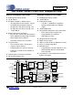
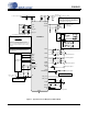
CS42L51 2. TYPICAL CONNECTION DIAGRAMS See Note 4 +1.8 V or +2.5 V 1 µF 0.1 µF 0.1 µF VD VA 0.1 µF +1.8 V or +2.5 V 1 µF Note 4: Series resistance in the path of the power supplies must be avoided. Any voltage drop on VA_HP will directly impact the negative charge pump supply (VSS_HP) and result in clipping on the audio output . VA_HP AOUTB ** 1.5 µF 1 µF ** Headphone Out Left & Right FLYP AOUTA FLYN 0.022 µF See Note 5 VSS_HP 1.5 µF ** 51.
CS42L51 See Note 4 +1.8V or +2.5V 1 µF 0.1 µF 0.1 µF VD VA +1.8V or +2.5V 1 µF 0.1 µF Note 4: Series resistance in the path of the power supplies (typically used for added filtering) must be avoided. Any voltage drop on VA_HP will directly impact the negative charge pump supply (VSS_HP) and result in clipping on the audio output . VA_HP AOUTB 1 µF AOUTA FLYN 1 µF Headphone Out Left & Right FLYP ** 0.022 µF 51.1 Ω VSS_HP ** GND_HP 470Ω C * *Use low ESR ceramic capacitors.
CS42L51 3. CHARACTERISTIC AND SPECIFICATION TABLES (All Min/Max characteristics and specifications are guaranteed over the Specified Operating Conditions. Typical performance characteristics and specifications are derived from measurements taken at nominal supply voltages and TA = 25° C.) SPECIFIED OPERATING CONDITIONS (AGND=DGND=0 V, all voltages with respect to ground.) Parameters Symbol Min Nom Max Units 1.65 2.37 1.65 2.37 1.65 2.37 1.65 2.37 3.14 1.8 2.5 1.8 2.5 1.8 2.5 1.8 2.5 3.3 1.89 2.
CS42L51 ANALOG INPUT CHARACTERISTICS (COMMERCIAL - CNZ) (Test Conditions (unless otherwise specified): Input sine wave (relative to digital full scale): 1 kHz through passive input filter; Measurement Bandwidth is 10 Hz to 20 kHz unless otherwise specified. Sample Frequency = 48 kHz) VA = 2.5 V (nominal) Min Typ Max Parameter (Note 5) VA = 1.
CS42L51 ANALOG INPUT CHARACTERISTICS (AUTOMOTIVE - DNZ) (Test Conditions (unless otherwise specified): Input sine wave (relative to full scale): 1 kHz through passive input filter; Measurement Bandwidth is 10 Hz to 20 kHz unless otherwise specified. Sample Frequency = 48 kHz) VA = 2.5 V (nominal) Min Typ Max Parameter (Note 5) VA = 1.
CS42L51 5. Referred to the typical full-scale voltage. Applies to all THD+N and Dynamic Range values in the table. 6. Measured between AINxx and AGND. ADC DIGITAL FILTER CHARACTERISTICS Parameter (Note 7) Min Typ Max Unit 0 - 0.4948 Fs -0.09 - 0.17 dB Stopband 0.6 - - Fs Stopband Attenuation 33 - - dB - 7.6/Fs - s Passband (Frequency Response) Passband Ripple Total Group Delay to -0.1 dB corner High-Pass Filter Characteristics (48 kHz Fs) Frequency Response -3.0 dB -0.
CS42L51 ANALOG OUTPUT CHARACTERISTICS (COMMERCIAL - CNZ) (Test conditions (unless otherwise specified): Input test signal is a full-scale 997 Hz sine wave; measurement bandwidth is 10 Hz to 20 kHz; Sample Frequency = 48 kHz; test load RL = 10 kΩ, CL = 10 pF for the line output (see Figure 3), and test load RL = 16 Ω, CL = 10 pF (see Figure 3) for the headphone output. HP_GAIN[2:0] = 011.) VA = 1.8V (nominal) VA = 2.
CS42L51 ANALOG OUTPUT CHARACTERISTICS (AUTOMOTIVE - DNZ) (Test conditions (unless otherwise specified): Input test signal is a full-scale 997 Hz sine wave; measurement bandwidth is 10 Hz to 20 kHz; Sample Frequency = 48 kHz and 96 kHz; test load RL = 10 kΩ, CL = 10 pF for the line output (see Figure 3), and test load RL = 16 Ω, CL = 10 pF (see Figure 3) for the headphone output. HP_GAIN[2:0] = 011.) VA = 2.5V (nominal) Min Typ Max Parameter (Note 8) VA = 1.
CS42L51 LINE OUTPUT VOLTAGE CHARACTERISTICS Test conditions (unless otherwise specified): Input test signal is a full-scale 997 Hz sine wave; measurement bandwidth is 10 Hz to 20 kHz; Sample Frequency = 48 kHz; test load RL = 10 kΩ, CL = 10 pF (see Figure 3). Parameter VA = 2.5V (nominal) Min Typ Max VA = 1.8V (nominal) Min Typ Max 1.95 - 2.15 - 1.41 - - - Unit AOUTx Voltage Into RL = 10 kΩ HP_GAIN[2:0] Analog Gain (G) 000 0.3959 001 0.4571 010 0.5111 011 (default) 0.6047 100 0.
CS42L51 HEADPHONE OUTPUT POWER CHARACTERISTICS Test conditions (unless otherwise specified): Input test signal is a full-scale 997 Hz sine wave; measurement bandwidth is 10 Hz to 20 kHz; Sample Frequency = 48 kHz; test load RL = 16 Ω, CL = 10 pF (see Figure 3). VA = 1.8V (nominal) Min Typ Max VA = 2.5V (nominal) Min Typ Max Parameter Unit AOUTx Power Into RL = 16 Ω HP_GAIN[2:0] Analog Gain (G) 000 0.3959 001 0.4571 010 0.5111 011 (default) 0.6047 100 0.7099 101 0.8399 110 1.0000 111 1.
CS42L51 COMBINED DAC INTERPOLATION & ON-CHIP ANALOG FILTER RESPONSE Parameter (Note 12) Frequency Response 10 Hz to 20 kHz Passband to -0.05 dB corner to -3 dB corner StopBand StopBand Attenuation (Note 13) Group Delay De-emphasis Error Fs = 32 kHz Fs = 44.1 kHz Fs = 48 kHz Min Typ Max Unit -0.01 - +0.08 dB 0 0 - 0.4780 0.4996 Fs Fs 0.5465 - - Fs 50 - - dB - 10.4/Fs - s - - +1.5/+0 +0.05/-0.25 -0.2/-0.4 dB dB dB Notes: 12. Response is clock dependent and will scale with Fs.
CS42L51 Parameters Symbol Min Fs - Max Units Master Mode (Note 17) Output Sample Rate (LRCK) All Speed Modes (Note 17) MCLK ----------------128 Hz 45 55 % - 64•Fs Hz 45 55 % td(MSB) - 52 ns SDOUT Setup Time Before SCLK Rising Edge ts(SDO-SK) 20 - ns SDOUT Hold Time After SCLK Rising Edge th(SK-SDO) 30 - ns SDIN Setup Time Before SCLK Rising Edge ts(SD-SK) 20 - ns th 20 - ns LRCK Duty Cycle 1/tP SCLK Frequency SCLK Duty Cycle LRCK Edge to SDOUT MSB Output Delay SD
CS42L51 SWITCHING SPECIFICATIONS - I²C® CONTROL PORT (Inputs: Logic 0 = DGND, Logic 1 = VL, SDA CL = 30 pF) Parameter Symbol Min Max Unit SCL Clock Frequency fscl - 100 kHz RESET Rising Edge to Start tirs 500 - ns Bus Free Time Between Transmissions tbuf 4.7 - µs Start Condition Hold Time (prior to first clock pulse) thdst 4.0 - µs Clock Low time tlow 4.7 - µs Clock High Time thigh 4.0 - µs Setup Time for Repeated Start Condition tsust 4.
CS42L51 SWITCHING CHARACTERISTICS - SPI™ CONTROL PORT (Inputs: Logic 0 = DGND, Logic 1 = VL) Parameter Symbol Min Max Units CCLK Clock Frequency fsck 0 6.0 MHz RESET Rising Edge to CS Falling tsrs 20 - ns CS Falling to CCLK Edge tcss 20 - ns CS High Time Between Transmissions tcsh 1.
CS42L51 DC ELECTRICAL CHARACTERISTICS (AGND = 0 V; all voltages with respect to ground.) Parameters Min Typ Max Units Nominal Voltage Output Impedance DC Current Source/Sink (Note 22) - 0.5•VA 23 - 10 V kΩ µA DAC_FILT+ Nominal Voltage ADC_FILT+ Nominal Voltage - VA VA - V V - -0.8•(VA_HP) 10 V µA 0.8•VA 0.7•VA 0.6•VA 0.
CS42L51 POWER CONSUMPTION See (Note 25) PDN_DACB PDN_DACA PDN_PGAB PDN_PGAA PDN_ADCB PDN_ADCA PDN PDN_MICB PDN_MICA PDN_MICBIAS Power Ctl. Registers 02h 03h Operation Typical Current (mA) iVA_HP iVA iVD iVL (Note 28) V Total Power (mWrms) 1 x x x x x x x x x x 1.8 2.5 0 0 0 0 0 Off (Note 26) 0 0 0 0 0 2 Standby (Note 27) x x x x x x 1 x x x 1.8 2.5 0 0.01 0.02 0 0.05 0 0.01 0.03 0 0.10 3 Mono Record ADC 1 1 1 1 1 0 0 1 1 1 1.8 2.5 PGA to ADC 1 1 1 0 1 0 0 1 1 1 1.
CS42L51 4. APPLICATIONS 4.1 4.1.1 Overview Architecture The CS42L51 is a highly integrated, low power, 24-bit audio CODEC comprised of stereo analog-to-digital converters (ADC), and stereo digital-to-analog converters (DAC) designed using multi-bit delta-sigma techniques. The DAC operates at an oversampling ratio of 128Fs and the ADC operates at 64Fs, where Fs is equal to the system sample rate. The different clock rates maximize power savings while maintaining high performance.
CS42L51 4.2 Hardware Mode A limited feature-set is available when the CODEC powers up in Hardware Mode (see “Recommended Power-Up Sequence” on page 41) and may be controlled via stand-alone control pins. Table 2 shows a list of functions/features, the default configuration and the associated stand-alone control available.
CS42L51 4.3 Analog Inputs AINxA and AINxB are the analog inputs, internally biased to VQ, that accepts line-level and MIC-level signals, allowing various gain and signal adjustments for each channel.
CS42L51 4.3.2 High-Pass Filter and DC Offset Calibration The high-pass filter continuously subtracts a measure of the DC offset from the output of the decimation filter. If the high-pass filter is “frozen” during normal operation, the current value of the DC offset for the corresponding channel is held. It is this DC offset that will continue to be subtracted from the conversion result. This feature makes it possible to perform a system DC offset calibration by: 1.
CS42L51 1 fc = ----------------------------------------------- = 3.18 Hz 2π ( 50 kΩ ) ( 1 µF ) The MICBIAS series resistor must be selected based on the requirements of the particular microphone used. The MICBIAS output pin is selected using the MICBIAS_SEL bit. Software Controls: “Interface Control (Address 04h)” on page 52, “MIC Control (Address 05h)” on page 53. MICBIAS 20 MICIN1 + // 17 Σ + // MICIN2 18 Figure 9. MIC Input Mix w/Common Mode Rejection 2.5 V 2.15 V VA AINxA 1.25 V 0.
CS42L51 4.3.5 Analog Input Multiplexer A stereo 4-to-1 analog input multiplexer selects between a line-level input source, or a mic-level input source, depending on the PDN_PGAx and AINx_MUX[1:0] bit settings. Signals may be routed to or bypassed around the PGA. To conserve power, the PGA’s may be powered down allowing the user to select from multiple line-level sources and route the stereo signal directly to the ADC. When using the MIC preamp, however, the PGA must be powered up.
CS42L51 4.3.7 Automatic Level Control (ALC) When enabled, the ALC monitors the analog input signal after the digital attenuator, detects when peak levels exceed the maximum threshold settings and lowers, first, the PGA gain settings and then increases the digital attenuation levels at a programmable attack rate and maintains the resulting level below the maximum threshold.
CS42L51 4.3.8 Noise Gate The noise gate may be used to mute signal levels that fall below a programmable threshold. This prevents the ALC from applying gain to noise. A programmable delay may be used to set the minimum time before the noise gate attacks the signal. Maximum noise gate attenuation levels will depend on the gain applied in either the PGA or MIC pre-amplifier.
CS42L51 4.4 Analog Outputs AOUTA and AOUTB are the ground-centered line or headphone outputs. Various signal processing options are available, including digital mixes with the ADC signal and an internal Beep Generator. The desired path to the DAC must be selected using the DATA_SEL[1:0] bits. Software Controls: “DAC Control (Address 09h)” on page 58. ARATE[7:0] RRATE[7:0] MAX[2:0] MIN[2:0] LIM_SRDIS LIM_ZCDIS LIMIT_EN SIGNAL PROCESSING ENGINE (SPE) OUTA_VOL[7:0] OUTB_VOL[7:0] +12dB/-102dB 0.
CS42L51 Gain dB T1=50 µs 0dB T2 = 15 µs -10dB F1 3.183 kHz F2 Frequency 10.61 kHz Figure 14. De-Emphasis Curve 4.4.2 Volume Controls Three digital volume control functions are implemented, offering independent control over the ADC and PCM signal paths into the mixer as well as a combined control over the mixed signals. All volume controls are programmable to ramp in increments of 0.125 dB at a rate controlled by the DAC soft ramp/zero cross settings.
CS42L51 REPEAT = '1' BEEP = '1' CONTINUOUS BEEP: Beep turns on at a configurable frequency (FREQ) and volume (BPVOL) and remains on until REPEAT is cleared. REPEAT = '1' BEEP = '0' MULTI-BEEP: Beep turns on at a configurable frequency (FREQ) and volume (BPVOL) for the duration of ONTIME and turns off for the duration of OFFTIME. On and off cycles are repeated until REPEAT is cleared.
CS42L51 Input MAX[2:0] Limiter AOUTx_VOL[7:0] volume control should NOT be adjusted manually when Limiter is enabled. ATTACK/RELEASE SOUND CUSHION Volume Output (after Limiter) CUSH[2:0] MAX[2:0] ARATE[5:0] RRATE[5:0] Figure 16. Peak Detect & Limiter 4.4.7 Line-Level Outputs and Filtering The CODEC contains on-chip buffer amplifiers capable of producing line level single-ended outputs on AOUTA and AOUTB. These amplifiers are ground centered and do not have any DC offset.
CS42L51 4.4.8 On-Chip Charge Pump An on-chip charge pump derives a negative supply voltage from the VA_HP supply. This provides dual rail supplies allowing a full-scale output swing centered around ground and eliminates the need for large, DC-blocking capacitors. Added benefits include greater pop suppression and improved low frequency (bass) response. Note: Series resistance in the path of the power supplies must be avoided.
CS42L51 4.5.1 Slave LRCK and SCLK are inputs in Slave Mode. The speed of the CODEC is automatically determined based on the input MCLK/LRCK ratio when the Auto-Detect function is enabled. Certain input clock ratios will then require an internal divide-by-two of MCLK* using either the MCLKDIV2 bit or the MCLKDIV2 standalone control pin. Additional clock ratios are allowed when the Auto-Detect function is disabled; but the appropriate speed mode must be selected using the SPEED[1:0] bits.
CS42L51 4.5.3 High-Impedance Digital Output The serial port may be placed on a clock/data bus that allows multiple masters for the serial port I/O without the need for external buffers. The 3ST_SP bit places the internal buffers for these I/O in a high-impedance state, allowing another device to transmit serial port data without bus contention. CS42L51 Transmitting Device #2 Transmitting Device #1 SDOUT 3ST_SP SCLK/LRCK Receiving Device Figure 18. Tri-State Serial Port 4.5.
CS42L51 LRCK L eft C h a n n e l R ig ht C h a n n e l SCLK SDIN MSB LS B MSB LSB MSB AOUTB / AINxB AOUTA / AINxA Figure 20. Left-Justified Format LRCK L eft C h a n n el R ig ht C h a n n el SCLK MSB SDIN M SB LSB AOUTA LS B AOUTB Figure 21. Right-Justified Format (DAC only) 4.7 Initialization The initialization and Power-Down sequence flowchart is shown in Figure 22 on page 42. The CODEC enters a Power-Down state upon initial power-up.
CS42L51 4.9 Recommended Power-Down Sequence To minimize audible pops when turning off or placing the CODEC in standby, 1. Mute the DAC’s and ADC’s. 2. Set the PDN bit in the power control register to ‘1’b. The CODEC will not power down until it reaches a fully muted sate. Do not remove MCLK until after the part has fully muted. Note that it may be necessary to disable the soft ramp and/or zero cross volume transitions to achieve faster muting/power down. 3. Bring RESET low. No Power 1.
CS42L51 4.10 Software Mode The control port is used to access the registers allowing the CODEC to be configured for the desired operational modes and formats. The operation of the control port may be completely asynchronous with respect to the audio sample rates. However, to avoid potential interference problems, the control port pins should remain static if no operation is required. The control port operates in two modes: SPI and I²C, with the CODEC acting as a slave device.
CS42L51 the contents of the register pointed to by the MAP will be output. Setting the auto-increment bit in MAP allows successive reads or writes of consecutive registers. Each byte is separated by an acknowledge bit. The ACK bit is output from the CS42L51 after each input byte is read and is input to the CS42L51 from the microcontroller after each transmitted byte.
CS42L51 4.10.3 Memory Address Pointer (MAP) The MAP byte comes after the address byte and selects the register to be read or written. Refer to the pseudo code above for implementation details. 4.10.3.1 Map Increment (INCR) The device has MAP auto-increment capability enabled by the INCR bit (the MSB) of the MAP. If INCR is set to 0, MAP will stay constant for successive I²C writes or reads and SPI writes.
CS42L51 5. REGISTER QUICK REFERENCE Software mode register defaults are as shown. “Reserved” registers must maintain their default state. Addr 01h Function ID p 49 default 02h Power Ctl. 1 p 49 default 03h Speed Ctl. & Power Ctl. 2 p 50 default 04h Interface Ctl. p 52 default 05h MIC Control & Misc.
CS42L51 Addr Function p 60 default 0Eh Vol. Control ADCMIXA p 61 default 0Fh Vol. Control ADCMIXB p 61 default 10h Vol. Control PCMMIXA p 62 default 11h Vol. Control PCMMIXB p 62 default 12h BEEP Freq. & OnTime p 62 default 13h BEEP Off Time & Vol. p 63 default 14h BEEP Control & Tone Config p 64 default 15h Tone Control p 65 default 16h Vol. Control AOUTA p 66 default 17h Vol.
CS42L51 Addr Function 7 6 5 4 3 2 1 0 1Ah Limiter Config & Release Rate LIMIT_EN LIMIT_ALL LIM_RRATE 5 LIM_RRATE 4 LIM_RRATE 3 LIM_RRATE 2 LIM_RRATE 1 LIM_RRATE 0 0 1 1 1 1 1 1 1 Reserved Reserved p 70 default 0 0 1Ch ALC Enable & Attack Rate ALC_ENB ALC_ENA p 70 default 0 0 1Dh ALC Release Rate Reserved Reserved p 71 default 0 0 1 1 1 1 1 1 MAX2 MAX1 MAX0 MIN2 MIN1 MIN0 Reserved Reserved 0 0 0 0 0 0 0 0 NG_ALL NG_EN NG_BOOST THRESH2 THR
CS42L51 6. REGISTER DESCRIPTION All registers are read/write except for the chip I.D. and Revision Register and Interrupt Status Register which are read only. See the following bit definition tables for bit assignment information. The default state of each bit after a power-up sequence or reset is listed in each bit description. All “Reserved” registers must maintain their default state.
CS42L51 Power Down PGA X (PDN_PGAX) Default: 0 0 - Disable 1 - Enable Function: PGA channel x will either enter a power-down or muted state when this bit is enabled. See Power Control 1 (Address 02h) on page 49 above. This bit is used in conjunction with AINx_MUX bits to determine the analog input path to the ADC. Refer to “ADCX Input Select Bits (AINX_MUX[1:0])” on page 56 for the required settings.
CS42L51 Speed Mode (SPEED[1:0]) Default: 01 11 - Quarter-Speed Mode (QSM) - 4 to 12.5 kHz sample rates 10 - Half-Speed Mode (HSM) - 12.5 to 25 kHz sample rates 01 - Single-Speed Mode (SSM) - 4 to 50 kHz sample rates 00 - Double-Speed Mode (DSM) - 50 to 100 kHz sample rates Function: Sets the appropriate speed mode for the CODEC in Master or Slave Mode. QSM is optimized for 8 kHz sample rate and HSM is optimized for 16 kHz sample rate.
CS42L51 6.4 Interface Control (Address 04h) 7 SDOUT->SDIN 6 M/S 5 DAC_DIF2 4 DAC_DIF1 3 DAC_DIF0 2 ADC_I²S/LJ 1 DIGMIX 0 MICMIX SDOUT to SDIN Loopback (SDOUT->SDIN) Default: 0 0 - Disabled; SDOUT internally disconnected from SDIN 1 - Enabled; SDOUT internally connected to SDIN Function: Internally loops the signal on the SDOUT pin to SDIN. Master/Slave Mode (M/S) Default: 0 0 - Slave 1 - Master Function: Selects either master or slave operation for the serial port.
CS42L51 ADC I²S or Left-Justified (ADC_I²S/LJ) Default: 0 0 - Left-Justified 1 - I²S Function: Selects either the I²S or Left-Justified digital interface format for the data on SDOUT. The required relationship between the Left/Right clock, serial clock and serial data is defined by the Digital Interface Format and the options are detailed in this section . Digital Mix (DIGMIX) Default: 0 DIGMIX 0 DATA_SEL[1:0] xx 00 01 10 11 1 Mix Selected No Mix: ADC to ADC serial port, SDOUT data.
CS42L51 ADCx 20 dB Digital Boost (ADCx_DBOOST) Default: 0 0 - Disabled 1 - Enabled Function: Applies a 20 dB digital gain to the input signal on ADC channel x, regardless of the input path. MIC Bias Select (MICBIAS_SEL) Default: 0 0 - MICBIAS on AIN3B/MICIN2 pin 1 - MICBIAS on AIN2B pin Function: Determines the output pin for the internally generated MICBIAS signal. If set to ‘0’b, the MICBIAS is output on the AIN3B/MICIN2 pin. If set to ‘1’b, the MICBIAS is output on the AIN2B pin.
CS42L51 ADCX High-Pass Filter Freeze (ADCX_HPFRZ) Default: 0 0 - Continuous DC Subtraction 1 - Frozen DC Subtraction Function: The high-pass filter works by continuously subtracting a measure of the DC offset from the output of the decimation filter. If the ADCx_HPFRZ bit is taken high during normal operation, the current value of the DC offset is frozen, and this DC offset will continue to be subtracted from the conversion result. For DC measurements, this bit must be set to ‘1’.
CS42L51 6.7 ADCx Input Select, Invert & Mute (Address 07h) 7 AINB_MUX1 6 AINB_MUX0 5 AINA_MUX1 4 AINA_MUX0 3 INV_ADCB 2 INV_ADCA 1 0 ADCB_MUTE ADCA_MUTE ADCX Input Select Bits (AINX_MUX[1:0]) Default: 00 PDN_PGAx AINx_MUX[1:0] 0 0 0 0 1 1 1 1 00 01 10 11 00 01 10 11 Selected Path to ADC AIN1x-->PGAx AIN2x-->PGAx AIN3x/MICINx-->PGAx AIN3x/MICINx-->Pre-Amp(+16/+32 dB Gain)-->PGAx AIN1x AIN2x AIN3x/MICINx Reserved Function: Selects the specified analog input signal into ADCx.
CS42L51 6.8 DAC Output Control (Address 08h) 7 6 5 HP_GAIN2 HP_GAIN1 HP_GAIN0 4 DAC_ SNGVOL 3 2 INV_PCMB INV_PCMA 1 0 DACB_MUTE DACA_MUTE Headphone Analog Gain (HP_GAIN[2:0]) Default: 011 HP_GAIN[2:0] Gain Setting 000 001 010 011 100 101 110 111 0.3959 0.4571 0.5111 0.6047 0.7099 0.8399 1.0000 1.1430 Function: These bits select the gain multiplier for the headphone/line outputs. See “Line Output Voltage Characteristics” on page 18 and “Headphone Output Power Characteristics” on page 19.
CS42L51 6.9 DAC Control (Address 09h) 7 DATA_SEL1 6 DATA_SEL0 5 FREEZE 4 Reserved 3 DEEMPH 2 AMUTE 1 DAC_SZC1 0 DAC_SZC0 DAC Data Selection (DATA_SEL[1:0]) Default: 00 00 - PCM Serial Port to DAC 01 - Signal Processing Engine to DAC 10 - ADC Serial Port to DAC 11 - Reserved Function: Selects the digital signal source for the DAC. Note: Certain functions are only available when the “Signal Processing Engine to DAC” option is selected using these bits.
CS42L51 DAC Soft Ramp and Zero Cross Control (DAC_SZC[1:0]) Default = 10 00 - Immediate Change 01 - Zero Cross 10 - Soft Ramp 11 - Soft Ramp on Zero Crossings Function: Note: The DATA_SEL[1:0] bits in reg09h must be set to ‘01’b to enable function control Immediate Change When Immediate Change is selected all volume-level changes will take effect immediately in one step.
CS42L51 ALCX Zero Cross Disable (ALCX_ZCDIS) Default: 0 0 - Off 1 - On Function: Overrides the ZCROSSx bit setting for the ADC. When this bit is set, the ALC attack rate in the PGA will not be dictated by the zero cross setting. ALC volume-level changes will take effect immediately in one step. PGA X Gain Control (PGAX_VOL[4:0]) Default: 00000 Binary Code Volume Setting 11000 ··· 01010 ··· 00000 11111 11110 ··· 11001 11010 +12 dB ··· +5 dB ··· 0 dB -0.
CS42L51 Function: The level of ADCX can be adjusted in 1.0 dB increments as dictated by the ADCx Soft and Zero Cross bits (SOFTx & ZCROSSx) from 0 to -96 dB. Levels are decoded in two’s complement, as shown in the table above. Note: 6.12 When the ALC is enabled, the Attenuator and PGA volume is automatically controlled and should not be adjusted manually.
CS42L51 6.13 PCMX Mixer Volume Control: PCMA (Address 10h) & PCMB (Address 11h) 7 MUTE_ PCMMIXx 6 PCMMIXx_ VOL6 5 PCMMIXx_ VOL5 4 PCMMIXx_ VOL4 3 PCMMIXx_ VOL3 2 PCMMIXx_ VOL2 1 PCMMIXx_ VOL1 0 PCMMIXx_ VOL0 Note: The DATA_SEL[1:0] bits in reg09h must be set to ‘01’b to enable function control in this register. PCMX Mixer Channel Mute (MUTE_PCMMIXX) Default = 1 0 - Disabled 1 - Enabled Function: The PCM channel X input to the output mixer will mute when enabled.
CS42L51 FREQ[3:0] Frequency Pitch Fs = 12, 24, 48 or 96 kHz 0101 0110 0111 1000 1001 1010 1011 1100 1101 1110 1111 774.19 Hz 888.89 Hz 1000.00 Hz 1043.48 Hz 1200.00 Hz 1333.33 Hz 1411.76 Hz 1600.00 Hz 1714.29 Hz 2000.00 Hz 2181.82 Hz G5 A5 B5 C6 D6 E6 F6 G6 A6 B6 C7 Function: The frequency of the beep signal can be adjusted from 260.87 Hz to 2181.82 Hz. Beep frequency will scale directly with sample rate, Fs, but is fixed at the nominal Fs within each speed mode.
CS42L51 OFFTIME[2:0] Off Time Fs = 12, 24, 48 or 96 kHz 110 111 9.35 s 10.80 s Function: The off-duration of the beep signal can be adjusted from approximately 75 ms to 680 ms. The off-duration will scale inversely with sample rate, Fs, but is fixed at the nominal Fs within each speed mode. Refer to Figure 15 on page 36 for single-, multiple- and continuous-beep configurations using the REPEAT and BEEP bits.
CS42L51 This bit is used in conjunction with the REPEAT bit to mix a continuous or periodic beep with the analog output. Note: Re-engaging the beep before it has completed its initial cycle will cause the beep signal to remain ON for the maximum ONTIME duration. Refer to Figure 15 on page 36 for a description of each configuration option. Treble Corner Frequency (TREB_CF[1:0]) Default: 00 00 - 5 kHz 01 - 7 kHz 10 - 10 kHz 11 - 15 kHz Function: The treble corner frequency is user selectable as shown above.
CS42L51 Function: The level of the shelving treble gain filter is set by Treble Gain Level. The level can be adjusted in 1.5 dB increments from +12.0 to -10.5 dB. Bass Gain Level (BASS[3:0]) Default: 1000 dB (No Bass Gain) Binary Code Gain Setting 0000 ··· 0111 1000 1001 ··· 1111 +12.0 dB ··· +1.5 dB 0 dB -1.5 dB ··· -10.5 dB Function: The level of the shelving bass gain filter is set by Bass Gain Level. The level can be adjusted in 1.5 dB increments from +10.5 to -10.5 dB. 6.
CS42L51 6.19 PCM Channel Mixer (Address 18h) 7 PCMA1 6 PCMA0 5 PCMB1 4 PCMB0 3 ADCA1 2 ADCA0 1 ADCB1 0 ADCB0 Note: The DATA_SEL[1:0] bits in reg09h must be set to ‘01’b to enable function control in this register.
CS42L51 Cushion Threshold (CUSH[2:0]) Default: 000 CUSH[2:0] Threshold Setting (dB) 000 0 001 -3 010 -6 011 -9 101 -12 101 -18 110 -24 111 -30 Function: Sets a cushion level below full scale. This setting is usually set slightly below the maximum (MAX[2:0]) threshold. The Limiter uses this cushion as a hysteresis point for the input signal as it maintains the signal below the maximum as well as below the cushion setting.
CS42L51 6.21 Limiter Release Rate Register (Address 1Ah) 7 LIMIT_EN 6 LIMIT_ALL 5 RRATE5 4 RRATE4 3 RRATE3 2 RRATE2 1 RRATE1 0 RRATE0 Note: The DATA_SEL[1:0] bits in reg09h must be set to ‘01’b to enable function control in this register. Peak Detect and Limiter Enable (LIMIT_EN) Default: 0 0 - Disabled 1 - Enabled Function: Limits the maximum signal amplitude to prevent clipping when this function is enabled. Peak Signal Limiting is performed by digital attenuation.
CS42L51 6.22 Limiter Attack Rate Register (Address 1Bh) 7 Reserved 6 Reserved 5 ARATE5 4 ARATE4 3 ARATE3 2 ARATE2 1 ARATE1 0 ARATE0 Note: The DATA_SEL[1:0] bits in reg09h must be set to ‘01’b to enable function control in this register.
CS42L51 6.24 ALC Release Rate (Address 1Dh) 7 Reserved 6 Reserved 5 4 3 2 1 0 ALC_RRATE5 ALC_RRATE4 ALC_RRATE3 ALC_RRATE2 ALC_RRATE1 ALC_RRATE0 ALC Release Rate (RRATE[5:0]) Default: 111111 Binary Code Release Time 000000 ··· 111111 Fastest Release ··· Slowest Release Function: Sets the rate at which the ALC releases the PGA & digital attenuation from levels below the minimum setting in the ALC threshold register, and returns the input level to the PGA_VOL[4:0] & ADCx_ATT[7:0] setting.
CS42L51 MIN[2:0] Threshold Setting (dB) 011 -9 100 -12 101 -18 110 -24 111 -30 Function: Sets the minimum level at which to disengage the ALC’s attenuation or amplify the input signal at a rate set in the release rate register until levels again reach this minimum threshold. The ALC uses this minimum as a hysteresis point for the input signal as it maintains the signal below the maximum as well as below the minimum setting. This provides a more natural sound as the ALC attacks and releases. 6.
CS42L51 Function: Sets the threshold level of the noise gate. Input signals below the threshold level will be attenuated to -96 dB. NG_BOOST = ‘1’b adds 30 dB to the threshold settings. Noise Gate Delay Timing (NGDELAY[1:0]) Default: 00 00 - 50 ms 01 - 100 ms 10 - 150 ms 11 - 200 ms Function: Sets the delay time before the noise gate attacks. Noise gate attenuation is dictated by the SOFTx & ZCROSS bit settings unless the disable bit for each function is enabled. 6.
CS42L51 6.28 Charge Pump Frequency (Address 21h) 7 6 5 4 CHRG_FREQ CHRG_FREQ CHRG_FREQ CHRG_FREQ 3 2 1 0 3 2 1 0 Reserved Reserved Reserved Reserved Charge Pump Frequency (CHRG_FREQ[3:0]) Default: 0101 N CHRG_FREQ[3:0] 0 ... 15 0000 ...
CS42L51 7. ANALOG PERFORMANCE PLOTS 7.1 Headphone THD+N versus Output Power Plots Test conditions (unless otherwise specified): Input test signal is a 997 Hz sine wave; measurement bandwidth is 10 Hz to 20 kHz; Fs = 48 kHz. Plots were taken from the CDB42L51 using an Audio Precision analyzer. -10 G = 0.6047 -15 VA_HP = VA = 1.8 V G = 0.7099 -20 G = 0.8399 -25 -30 G = 1.0000 -35 G = 1.1430 -40 Legend -45 d B r A -50 NOTE: Graph shows the output power per channel (i.e.
CS42L51 G = 0.6047 VA_HP = VA = 1.8 G = 0.7099 -20 -30 G = 0.8399 -35 G = 1.0000 -40 G = 1.1430 -45 Legend -50 NOTE: Graph shows the output power per channel (i.e. Output Power = 22 mW into single 32 Ω and 44 mW into stereo 32 Ω with THD+N = 75 dB). -55 d B r -60 A -65 -70 -75 -80 -85 -90 -95 -100 0 6m 12m 18m 24m 30m 36m 42m 48m 54m 60m W Figure 29. THD+N vs. Output Power per Channel at 1.8 V (32 Ω load) G = 0.6047 -20 VA_HP = VA = 2.5 V -25 G = 0.7099 -30 G = 0.
CS42L51 7.2 Headphone Amplifier Efficiency The architecture of the headphone amplifier is that of typical class AB amplifiers. Test conditions (unless otherwise specified): Input test signal is a 997 Hz sine wave; Power Consumption Mode 6 - Stereo Playback w/16 Ω load. HP_GAIN = 1.1430. Best efficiency is realized when the amplifier outputs maximum power. VA_HP = VA = 1.8 V Figure 31. Power Dissipation vs. Output Power into Stereo 16 Ω VA_HP = VA = 1.8 V Figure 32. Power Dissipation vs.
CS42L51 7.3 ADC_FILT+ Capacitor Effects on THD+N The value of the capacitor on the ADC_FILT+ pin, 16, affects the low frequency total harmonic distortion + noise (THD+N) performance of the ADC. Larger capacitor values yield significant improvement in THD+N at low frequencies. Figure 33 shows the THD+N versus frequency for the ADC analog input. Plots were taken from the CDB42L51 using an Audio Precision analyzer.
CS42L51 8. EXAMPLE SYSTEM CLOCK FREQUENCIES 8.1 Auto Detect Enabled Sample Rate LRCK (kHz) 1024x MCLK (MHz) 1536x 2048x* 8 11.025 12 3072x* 8.1920 11.2896 12.2880 12.2880 16.9344 18.4320 24.5760 33.8688 36.8640 Sample Rate LRCK (kHz) 512x MCLK (MHz) 768x 1024x* 16 22.05 24 8.1920 11.2896 12.2880 12.2880 16.9344 18.4320 16.3840 22.5792 24.5760 16.3840 22.5792 24.5760 Sample Rate LRCK (kHz) MCLK (MHz) 384x 512x* 256x 32 44.1 48 8.1920 11.2896 12.2880 12.2880 16.9344 18.
CS42L51 8.2 80 Auto Detect Disabled Sample Rate LRCK (kHz) 512x 8 11.025 12 6.1440 768x MCLK (MHz) 1024x 1536x 2048x 3072x 6.1440 8.4672 9.2160 8.1920 11.2896 12.2880 16.3840 22.5792 24.5760 24.5760 33.8688 36.8640 Sample Rate LRCK (kHz) 256x 384x 512x 16 22.05 24 6.1440 6.1440 8.4672 9.2160 8.1920 11.2896 12.2880 12.2880 16.9344 18.4320 MCLK (MHz) 768x 12.2880 16.9344 18.4320 Sample Rate LRCK (kHz) 256x 32 44.1 48 8.1920 11.2896 12.2880 12.2880 16.9344 18.
CS42L51 9. PCB LAYOUT CONSIDERATIONS 9.1 Power Supply, Grounding As with any high-resolution converter, the CS42L51 requires careful attention to power supply and grounding arrangements if its potential performance is to be realized. Figure 1 on page 10 shows the recommended power arrangements, with VA and VA_HP connected to clean supplies. VD, which powers the digital circuitry, may be run from the system logic supply. Alternatively, VD may be powered from the analog supply via a ferrite bead.
CS42L51 10.ADC & DAC DIGITAL FILTERS 82 Figure 34. ADC Passband Ripple Figure 35. ADC Stopband Rejection Figure 36. ADC Transition Band Figure 37. ADC Transition Band Detail Figure 38. DAC Passband Ripple Figure 39. DAC Stopband Figure 40. DAC Transition Band Figure 41.
CS42L51 11.PARAMETER DEFINITIONS Dynamic Range The ratio of the rms value of the signal to the rms sum of all other spectral components over the specified bandwidth. Dynamic Range is a signal-to-noise ratio measurement over the specified band width made with a -60 dBFS signal. 60 dB is added to resulting measurement to refer the measurement to full-scale. This technique ensures that the distortion components are below the noise level and do not affect the measurement.
CS42L51 12.PACKAGE DIMENSIONS 32L QFN (5 X 5 mm BODY) PACKAGE DRAWING e b D Pin #1 Corner Pin #1 Corner E2 E A1 L D2 A Top View DIM MIN A A1 b D D2 E E2 e L -0.0000 0.0071 0.1280 0.1280 0.0118 Bottom View Side View INCHES NOM --0.0091 0.1969 BSC 0.1299 0.1969 BSC 0.1299 0.0197 BSC 0.0157 MAX MIN 0.0394 0.0020 0.0110 -0.00 0.18 0.1319 3.25 0.1319 3.25 0.0197 0.30 MILLIMETERS NOM --0.23 5.00 BSC 3.30 5.00 BSC 3.30 0.50 BSC 0.40 NOTE MAX 1.00 0.05 0.28 3.35 3.35 0.
CS42L51 13.ORDERING INFORMATION Product CS42L51 CDB42L51 CRD42L51 Description Low-Power Stereo CODEC w/HP Amp for Portable Apps CS42L51 Evaluation Board CS42L51 Reference Design Package Pb-Free Grade Temp Range Commercial -10 to +70° C 32L-QFN Yes Automotive -40 to +85° C Container Order # Rail CS42L51-CNZ Tape & Reel CS42L51-CNZR Rail CS42L51-DNZ Tape & Reel CS42L51-DNZR - No - - - CDB42L51 - No - - - CRD42L51 14.REFERENCES 1.
CS42L51 15.REVISION HISTORY Revision 86 Changes A1 Initial Release A2 Renamed pin 14, FILT1+, to DAC_FILT+ and pin 16, FILT2+, to ADC_FILT+. Added 1.5 µF capacitor recommendation to figure “Typical Connection Diagram (Software Mode)” on page 10. Removed the 0.1µF capacitors from pins DAC_FILT+, ADC_FILT+ and VQ on the figures “Typical Connection Diagram (Software Mode)” on page 10 and “Typical Connection Diagram (Hardware Mode)” on page 11.
CS42L51 Revision Changes PP1 Adjusted the minimum voltage specification in “Specified Operating Conditions” section on page 12. Adjusted Ambient Operating Temp. specification in “Absolute Maximum Ratings” section on page 12. Adjusted maximum “Analog In to PGA to ADC” THD+N performance specification in “Analog Input Characteristics (Commercial - CNZ)” on page 13.
CS42L51 Contacting Cirrus Logic Support For all product questions and inquiries, contact a Cirrus Logic Sales Representative. To find the one nearest to you, go to www.cirrus.com. IMPORTANT NOTICE Cirrus Logic, Inc. and its subsidiaries ("Cirrus") believe that the information contained in this document is accurate and reliable. However, the information is subject to change without notice and is provided "AS IS" without warranty of any kind (express or implied).