
User guide

DS686F1 9
CS4270
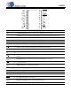
DAC ANALOG CHARACTERISTICS
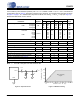
Test Conditions (unless otherwise specified): VD = VL = 3.3 V, AGND = DGND = 0 V; T
A
= +25° C; Full-Scale Out-
put Sine Wave, 997 Hz (Note 3). Decoupling capacitors, filter capacitors, and recommended output filter as shown
in Figure 1 on page 7. Fs = 48/96/192 kHz; Synchronous Mode; Test load R
L
= 3 k, C
L
= 10 pF (see Figure 2).
Measurement Bandwidth 10 Hz to 20 kHz.
Note: 3. One LSB of triangular PDF dither added to data.
Parameter Symbol
VA = 5 V VA = 3.3 V
UnitMin Typ Max Min Typ Max
Dynamic Range 18 to 24 bit A-weighted
unweighted
16 Bit A-weighted
unweighted
DR
99
96
90
87
105
102
96
93
-
-
-
-
97
94
90
87
103
100
96
93
-
-
-
-
dB
dB
dB
dB
Total Harmonic Distortion + Noise
18 to 24 bit 0 dB
-20 dB
-60 dB
16 Bit 0 dB
-20 dB
-60 dB
THD+N
-
-
-
-
-
-
-87
-82
-42
-85
-76
-36
-83
-
-
-81
-
-
-
-
-
-
-
-
-83
-80
-40
-81
-76
-36
-79
-
-
-77
-
-
dB
dB
dB
dB
dB
dB
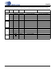
DAC Performance across Full VA Range
Parameter Symbol Min Typ Max Unit
Interchannel Isolation (1 kHz) - 100 - dB
DC Accuracy
Interchannel Gain Mismatch - 0.1 0.25 dB
Gain Drift -100 - +100 ppm/°C
Analog Output
Full Scale Output Voltage 0.6•VA 0.65•VA 0.7•VA Vpp
Max DC Current draw from AOUTA or AOUTB I
OUTmax
-10-A
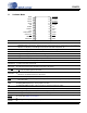
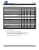
Max AC-Load Resistance (see Figure 3)R
L
-3-k
Max Load Capacitance (see Figure 3)C
L
-100-pF
Output Impedance of AOUTA and AOUTB Z
OUT
-100-
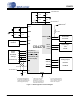
AOUTx
AGND
3.3 µF
V
out
R
L
C
L
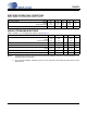
100
50
75
25
2.5
51015
Safe Operating
Region
Capacitive Load -- C (pF)
L
Resistive Load -- R (k
)
L
125
3
20
Figure 2. Output Test Load Figure 3. Maximum Loading