
User guide
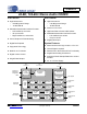

6 DS686F1
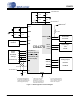
CS4270
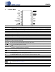
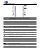
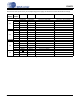
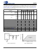
2. DIGITAL I/O PIN CHARACTERISTICS
The level for each input is set by its corresponding power supply and should not exceed the maximum ratings.
Power
Supply
Pin
Number
Pin Name I/O Driver Receiver
Software Mode
VLC
9 SDA/CDOUT Input/Output 1.8 V-5.0 V, Open Drain 1.8 V-5.0 V, with hysteresis
10 SCL/CCLK Input - 1.8 V-5.0 V, with hysteresis
11 AD0/CS Input - 1.8 V-5.0 V
12 AD1/CDIN Input - 1.8 V-5.0 V
13 AD2 Input - 1.8 V-5.0 V
Stand-Alone Mode
VLC
9 M1 Input - 1.8 V-5.0 V
10 M0 Input - 1.8 V-5.0 V
11 I²S/LJ Input - 1.8 V-5.0 V
12 MDIV1 Input - 1.8 V-5.0 V
13 MDIV2 Input - 1.8 V-5.0 V
All Modes
VD
1 SDIN Input - 3.3 V-5.0 V
2 LRCK Input/Output 3.3 V-5.0 V, CMOS 3.3 V-5.0 V
3 MCLK Input - 3.3 V-5.0 V
4 SCLK Input/Output 3.3 V-5.0 V, CMOS 3.3 V-5.0 V
7 SDOUT Output 3.3 V-5.0 V, CMOS -
VA
14 RST
Input - 1.8 V-5.0 V
21 MUTEA Output 3.3 V-5.0 V, CMOS -
24 MUTEB
Output 3.3 V-5.0 V, CMOS -
Table 1. Digital I/O Pin Power Rails