
User guide

44 DS686F1
CS4270
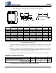
12.ORDERING INFORMATION
13.REVISION HISTORY
Product Description Package Pb-Free Temp Range Container Order #
CS4270 24-Bit 192 kHz Stereo Audio CODEC 24-TSSOP YES -10° to +70° C
Rail CS4270-CZZ
Tape & Reel CS4270-CZZR
CDB4270 CS4270 Evaluation Board -- - -CDB4270
Release Changes
F1
– Deleted automotive grade content and references to grade throughout.
– Formatting changes throughout.
– Updated several “Pin Descriptions” on page 4.
– Added “Digital I/O Pin Characteristics” on page 6.
– Added decoupling cap to VLC on Typical Connection Diagram, Figure 1 on page 7.
– Performance specifications updated per measured data in Section 4. “Characteristics and
Specifications” on page 8:
–Min Specified Operating Conditions for “DC Power Supplies:” on page 8.
– Typ and Max DAC Analog Characteristics for “Total Harmonic Distortion + Noise” on page 9.
–Max ADC Analog Characteristics for “Total Harmonic Distortion + Noise” on page 11.
– Typ ADC Analog Characteristics for “Interchannel Isolation” on page 11.
– Typ and Max DC Electrical Characteristics for “Power Supply Current” on page 13.
– Typ and Max DC Electrical Characteristics for “Power Consumption VA = 5 V, VD = VLC=
3.3 V” on page 13.
– Typ DC Electrical Characteristics for “FILT+ Output Impedance” on page 13.
–Min Switching Characteristics - Software Mode - SPI Format for "CCLK High Time" and
“CCLK Low Time” on page 18.
– Added “Acknowledge Delay from SCL Falling” on page 17.
– Added Transition Time from CCLK to CDOUT Valid (Note 21) and Time from CS rising to CDOUT
High-Z to “Switching Characteristics - Software Mode - SPI Format” on page 18.
– Added CDOUT to Figure 13 on page 18.
– Added Table 2 on page 19 and associated text in Section 5.1.1 Access to Stand-Alone Mode.
– Added Note 22 on page 20.
– Updated descriptions of recommended power-up sequences in “Serial Control Port Mode” on
page 21.
– Updated “Clock Ratio Selection” on page 22 (added all SCLK/LRCK ratios to the serial control
port mode table).
– Updated Section 5.2.7 “DC Offset Calibration Using the High-Pass Filter” on page 23.
– Added Section 5.3 “Popguard Transient Control” on page 24.
– Updated Section 5.5.1 “Input Component Values” on page 25
.
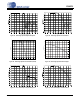
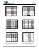
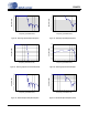
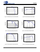
– Updated presentation of input source resistance plots (Figure 16 and Figure 17 on page 26).
– Added Section 6.2.2 SPI Read on page 30.
– Updated bit names in Section 7. “Register Quick Reference” on page 31.
– Updated Section 8.3.2 “Ratio Select (Bits 3:1)” on page 33.
– Updated Section 8.3.3 “Popguard Transient Control (Bit 0)” on page 33.
– Updated Section 8.4.1 and Section 8.4.2 on page 34.
– Updated Section 8.5.4 “De-Emphasis Control (Bit 0)” on page 36.