
User guide

30 DS686F1
CS4270
1. Bring CS low.
2. The address byte on the CDIN pin must then be 10011110 (R/W
=0).
3. Write to the memory address pointer, MAP. This byte points to the register to be written.
4. Write the desired data to the register pointed to by the MAP.
5. If the INCR bit (see Section 6.2.3.1) is set to 1, repeat the previous step until all the desired registers
are written, then bring CS high.
6. If the INCR bit is set to 0 and further SPI writes to other registers are desired, it is necessary to bring
CS
high, and follow the procedure detailed from step 1. If no further writes to other registers are
desired, bring CS
high
6.2.2 SPI Read
To read from the device, use the following procedure while adhering to the values specified in “Switching
Characteristics - Software Mode - SPI Format” section on page 18.
1. Bring CS
low.
2. The address byte on the CDIN pin must then be 10011111 (R/W
=1).
3. CDOUT pin will then output the data from the register pointed to by the MAP, which is set during the
SPI write operation.
4. If the INCR bit (see Section 6.2.3.1) is set to 1, keep CS
low and continue providing clocks on CCLK
to read from multiple consecutive registers. Bring CS
high when reading is complete.
5. If the INCR bit is set to 0 and further SPI reads from other registers are desired, it is necessary to bring
CS
high, and follow the procedure detailed from step 1. If no further reads from other registers are
desired, bring CS
high.
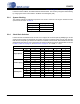
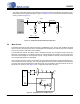
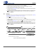
MAP
MSB
LSB
DATA
byte 1
byte n
R/W
R/W
ADDRESS
CHIP
ADDRESS
CHIP
MSB
LSB
MSB
LSB
MAP = Memory Address Pointer, 8 bits, MSB first
High Impedance
1001111 1001111
CCLK
CDIN
CDOUT
CS
Figure 22. Software Mode Timing, SPI Mode