
User guide

DS686F1 29
CS4270
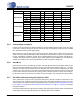
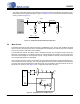
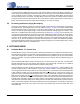
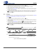
Since the read operation can not set the MAP, an aborted write operation is used as a preamble. As shown
in Figure 21, the write operation is aborted after the acknowledge for the MAP byte by sending a stop con-
dition. The following pseudocode illustrates an aborted write operation followed by a read operation.
Send start condition.
Send 10011xx0 (chip address & write operation).
Receive acknowledge bit.
Send MAP byte, auto increment off.
Receive acknowledge bit.
Send stop condition, aborting write.
Send start condition.
Send 10011xx1(chip address & read operation).
Receive acknowledge bit.
Receive byte, contents of selected register.
Send acknowledge bit.
Send stop condition.
Setting the auto increment bit in the MAP allows successive reads or writes of consecutive registers. Each
byte is separated by an acknowledge bit.
6.2 Software Mode - SPI Control Port
In SPI Mode, data is clocked into the serial control data line, CDIN, by the serial clock, CCLK (see Figure 22
for the clock to data relationship). There are no AD0 or AD1 pins. Pin CS
is the chip select signal and is
used to control SPI writes to the registers. When the device detects a high-to-low transition on the AD0/CS
pin after power-up, SPI Mode will be selected. All signals are inputs and data is clocked in on the rising edge
of CCLK.
6.2.1 SPI Write
To write to the device, use the following procedure while adhering to the Software Mode switching spec-
ifications in “Switching Characteristics - Software Mode - SPI Format” section on page 18.
4 5 6 7 24 25
SCL
CHIP ADDRESS (WRITE) MAP BYTE DATA
DATA +1
START
ACK
STOP
ACKACKACK
1 0 0 1 1 AD1 AD0 0
SDA
INCR 6 5 4 3 2 1 0 7 6 1 0 7 6 1 0 7 6 1 0
0 1 2 3 8 9 12 16 17 18 1910 11 13 14 15 27 28
26
DATA +n
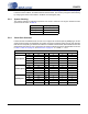
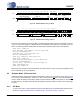
Figure 20. Software Mode Timing, I²C Write
SCL
CHIP ADDRESS (WRITE)
MAP BYTE
DATA
DATA +1
START
ACK
STOP
ACK
ACK
ACK
1 0 0 1 0 AD1 AD0 0
SDA
1 0 0 1 0 AD1 AD0 1
CHIP ADDRESS (READ)
START
INCR 6 5 4 3 2 1 0
7 0 7 0 7 0
NO
168 9 12 13 14 154 5 6 7 0 1 20 21 22 23 24
26 27 28
2 3 10 11 17 18 19 25
ACK
DATA + n
STOP
Figure 21. Software Mode Timing, I²C Read