
User guide

18 DS686F1
CS4270
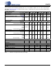
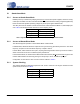
SWITCHING CHARACTERISTICS - SOFTWARE MODE - SPI FORMAT
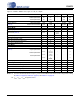
Inputs: Logic ‘0’ = AGND = DGND = 0 V; Logic ‘1’ = VLC; C
L
=20pF.
Notes: 18. t
spi
only needed before first falling edge of CS after RST rising edge. t
spi
= 0 at all other times.
19. Data must be held for sufficient time to bridge the transition time of CCLK.
20. For F
SCK
< 1 MHz.
21. CDOUT should not be sampled during this time.
Figure 13. SPI Control Port Timing
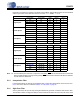
Parameter Symbol Min Max Unit
CCLK Clock Frequency f
sclk
-6MHz
RST Rising Edge to CS Falling t
srs
500 - ns
CCLK Edge to CS
Falling (Note 18) t
spi
500 - ns
CS
High Time Between Transmissions t
csh
1.0 - µs
CS Falling to CCLK Edge t
css
20 - ns
CCLK Low Time t
scl
66 - ns
CCLK High Time t
sch
66 - ns
CDIN to CCLK Rising Setup Time t
dsu
40 - ns
CCLK Rising to DATA Hold Time (Note 19) t
dh
15 - ns
Rise Time of CCLK and CDIN (Note 20) t
r2
- 100 ns
Fall Time of CCLK and CDIN (Note 20) t
f2
- 100 ns
Transition Time from CCLK to CDOUT Valid (Note 21) t
scdov
- 100 ns
Time from CS
rising to CDOUT High-Z t
cscdo
- 100 ns
t
r2
t
f2
t
dsu
t
dh
t
sch
t
scl
CS
CCLK
CDIN
t
css
t
csh
t
spi
t
srs
RST
CDOUT
t
scdov
t
scdov
t
cscdo
Hi-Impedance