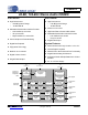
CS4270 24-Bit, 192-kHz Stereo Audio CODEC D/A Features A/D Features High Performance High Performance – – – – 105 dB Dynamic Range -87 dB THD+N Selectable Serial Audio Interface Formats – – – Multi-bit Conversion High-Pass Filter to Remove DC Offsets Left-Justified up to 24 bits I²S up to 24 bits Right-Justified 16, and 24 bits Selectable Serial Audio Interface Formats – – Control Output for External Muting Left-Justified up to 24 bits I²S up to 24 bits Single-Ended Input
CS4270 Stand-Alone Mode Feature Set System Features – Master or Slave Serial Audio Interface – Single-, Double-, or Quad-Speed Operation D/A Features – Auto-Mute on Static Samples – 44.
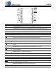
CS4270 TABLE OF CONTENTS 1. PIN DESCRIPTIONS .............................................................................................................................. 4 1.1 Software Mode ................................................................................................................................ 4 1.2 Stand-Alone Mode ........................................................................................................................... 5 2. DIGITAL I/O PIN CHARACTERISTICS .......
CS4270 1. PIN DESCRIPTIONS 1.1 Software Mode SDIN LRCK MCLK SCLK VD DGND SDOUT VLC SDA/CDOUT SCL/CCLK AD0/CS AD1/CDIN Pin Name # 1 24 2 23 3 22 4 21 5 20 6 19 7 18 8 17 9 16 10 15 11 14 12 13 MUTEB AOUTB AOUTA MUTEA AGND VA FILT+ VQ AINB AINA RST AD2 Pin Description SDIN 1 Serial Audio Data Input (Input) - Input for two’s complement serial audio data. LRCK 2 MCLK 3 Master Clock (Input) - Clock for the delta-sigma modulator and the digital filters.
CS4270 1.2 Stand-Alone Mode SDIN LRCK MCLK SCLK VD DGND SDOUT VLC M1 M0 I²S/LJ MDIV1 Pin Name # 1 24 2 23 3 22 4 21 5 20 6 19 7 18 8 17 9 16 10 15 11 14 12 13 MUTEB AOUTB AOUTA MUTEA AGND VA FILT+ VQ AINB AINA RST MDIV2 Pin Description SDIN 1 Serial Audio Data Input (Input) - Input for two’s complement serial audio data. LRCK 2 Left Right Clock (Input/Output) - Determines which channel, Left or Right, is currently active on the serialaudio data line.
CS4270 2. DIGITAL I/O PIN CHARACTERISTICS The level for each input is set by its corresponding power supply and should not exceed the maximum ratings. Power Pin Supply Number Software Mode VLC Pin Name I/O Driver Receiver 9 SDA/CDOUT Input/Output 1.8 V-5.0 V, Open Drain 1.8 V-5.0 V, with hysteresis 10 SCL/CCLK Input - 1.8 V-5.0 V, with hysteresis 11 AD0/CS Input - 1.8 V-5.0 V 12 AD1/CDIN Input - 1.8 V-5.0 V 13 AD2 Input - 1.8 V-5.0 V M1 Input - 1.8 V-5.
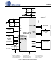
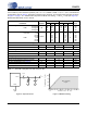
CS4270 3. TYPICAL CONNECTION DIAGRAM +3.3 V to 5 V 1 0.1 µF 1 µF 0.1 µF 1 µF 5.1 1 2 VD VA FILT+ 47 µF +3.3 V to 5 V GND or VD 0.1 µF 47 k AGND 10 µF 0.1 µF SDOUT (M/ S) SDIN VQ Analog Input Audio Data Processor AINA Network AINB CS4270 MCLK Timing Logic and Clocks SCLK LRCK AD2 (MDIV1) AD1/CDIN (MDIV2) Power Down and Mode Settings AD0 / CS (I2S/LJ) SDA/CDOUT (M1) SCL/CCLK (M0) (Control Port) 3 2 k 2 k and Mute VLC DGND 0.1 µF 1. Network AOUTB MUTEB 3 +1.
CS4270 4. CHARACTERISTICS AND SPECIFICATIONS SPECIFIED OPERATING CONDITIONS AGND = DGND= 0 V; all voltages with respect to ground. Parameters DC Power Supplies: Symbol Min Nom Max Units VA VD VLC TA 3.14 3.14 1.71 -40 5.0 3.3 3.3 - 5.25 5.25 5.25 +85 V V V C Analog Digital Serial Control Port Ambient Operating Temperature (Power Applied) ABSOLUTE MAXIMUM RATINGS AGND = DGND = 0 V, All voltages with respect to ground.
CS4270 DAC ANALOG CHARACTERISTICS Test Conditions (unless otherwise specified): VD = VL = 3.3 V, AGND = DGND = 0 V; TA = +25° C; Full-Scale Output Sine Wave, 997 Hz (Note 3). Decoupling capacitors, filter capacitors, and recommended output filter as shown in Figure 1 on page 7. Fs = 48/96/192 kHz; Synchronous Mode; Test load RL = 3 k, CL = 10 pF (see Figure 2). Measurement Bandwidth 10 Hz to 20 kHz.
CS4270 DAC COMBINED INTERPOLATION & ANALOG FILTER RESPONSE The filter characteristics have been normalized to the sample rate (Fs) and can be referenced to the desired sample rate by multiplying the given characteristic by Fs. (See Note 4) Parameter Symbol Min Typ Max Unit 0 0 - .35 .4992 Fs Fs Frequency Response 10 Hz to 20 kHz -.175 - +.01 dB StopBand .5465 - - Fs Single-Speed Mode Passband (Note 5) StopBand Attenuation to -0.
CS4270 ADC ANALOG CHARACTERISTICS Test Conditions (unless otherwise specified): VD = VL = 3.3 V, DGND = AGND = 0 V; TA = 25° C; 997 Hz Input Sine Wave. Figure 15 on page 26 shows the test circuit; Fs = 48/96/192 kHz; Synchronous Mode; Measurement Bandwidth 10 Hz to 20 kHz. Dynamic Performance Single-Speed Mode Dynamic Range Total Harmonic Distortion + Noise Double-Speed Mode VA = 5 V Fs = 48 kHz Symbol A-weighted unweighted (Note 8) -1 dB THD+N -20 dB -60 dB VA = 3.
CS4270 ADC DIGITAL FILTER CHARACTERISTICS Measurement Bandwidth is 10 Hz to 20 kHz unless otherwise specified. (Note 9) Parameter Symbol Min Typ Max Unit (Note 10) 0 - 0.49 Fs - - 0.035 dB (Note 10) 0.57 - - Fs 70 - - dB - 12/Fs - s 0 - 0.49 Fs - - 0.05 dB 0.56 - - Fs 69 - - dB - 9/Fs - s 0 - 0.26 Fs - - 0.05 dB 0.50 - - Fs 60 - - dB - 5/Fs - s Single-Speed Mode Passband (-0.
CS4270 DC ELECTRICAL CHARACTERISTICS TA = 25° C; AGND = DGND = 0 V, all voltages with respect to 0 V; MCLK = 12.288 MHz; Master Mode). Parameter Symbol Min Typ Max Unit VA = 5 V VA = 3.3 V VD, VLC = 5 V VD, VLC = 3.
CS4270 SWITCHING CHARACTERISTICS - SERIAL AUDIO INTERFACE Logic "0" = DGND = AGND = 0 V; Logic "1" = VD, CL = 20 pF. Parameter Sample Rate Single-Speed Mode Double-Speed Mode Quad-Speed Mode Symbol Min Typ Max Unit Fs Fs Fs 4 50 100 - 54 108 216 kHz kHz kHz fmclk fmclk 1.024 1.024 - 55.296 55.
CS4270 LRCK output LRCK input t mslr t slrd SCLK output SCLK input t sclkh t sdo SDOUT MSB MSB-1 MSB-2 t stp t hld MSB-3 SDOUT Figure 4. Master Mode, Left-Justified SAI MSB MSB-1 Figure 5. Slave Mode, Left-Justified SAI LRCK input LRCK output t slrd tmslr SCLK input SCLK output t sclkh MSB MSB-1 t sclkl t stp t hld t sdo SDOUT t sclkl SDOUT MSB-2 MSB-3 Figure 6. Master Mode, I²S SAI MSB Figure 7. Slave Mode, I²S SAI t sclkw SCLK t sdis t sdih SDIN Figure 8.
CS4270 Channel A - Left LRCK Channel B - Right SCLK SDATA MSB -1 -2 -3 -4 -5 +5 +4 +3 +2 +1 LSB MSB -1 -2 -3 -4 +5 +4 +3 +2 +1 LSB Figure 9. Format 0, Left-Justified up to 24-Bit Data Channel A - Left LRCK Channel B - Right SCLK SDINx MSB -1 -2 -3 -4 -5 +5 +4 +3 +2 +1 LSB MSB -1 -2 -3 -4 +5 +4 +3 +2 +1 LSB Figure 10.
CS4270 SWITCHING CHARACTERISTICS - SOFTWARE MODE - I²C FORMAT Inputs: Logic ‘0’ = AGND = DGND = 0 V, Logic ‘1’ = VLC, CL = 30 pF Parameter Symbol Min Max Unit SCL Clock Frequency fscl - 100 kHz RST Rising Edge to Start tirs 500 - ns Bus Free Time Between Transmissions tbuf 4.7 - µs Start Condition Hold Time (prior to first clock pulse) thdst 4.0 - µs Clock Low time tlow 4.7 - µs Clock High Time thigh 4.0 - µs Setup Time for Repeated Start Condition tsust 4.
CS4270 SWITCHING CHARACTERISTICS - SOFTWARE MODE - SPI FORMAT Inputs: Logic ‘0’ = AGND = DGND = 0 V; Logic ‘1’ = VLC; CL = 20 pF. Parameter Symbol Min Max Unit CCLK Clock Frequency fsclk - 6 MHz RST Rising Edge to CS Falling tsrs 500 - ns CCLK Edge to CS Falling (Note 18) tspi 500 - ns CS High Time Between Transmissions tcsh 1.
CS4270 5. APPLICATIONS 5.1 Stand-Alone Mode 5.1.1 Access to Stand-Alone Mode Reliable power-up is achieved by keeping the device in reset until the power supplies, clocks and configuration pins are stable. It is also recommended that RST be asserted if the analog or digital supplies drop below the minimum specified operating voltages to prevent power glitch related issues. The delay time from the release of reset until the device enters Stand-Alone Mode is 1,045 sample periods.
CS4270 5.1.4 Clock Ratio Selection Depending on whether the CS4270 is in Master or Slave Mode, different MCLK/LRCK and SCLK/LRCK ratios may be used. These ratios are shown in the Table 4. ‘0’ = DGND, ‘1’ = VLC.
CS4270 could result in recording a DC level, possibly yielding "clicks" when switching between devices in a multichannel system. In Stand-Alone Mode, the high-pass filter is always active and continuously subtracts a measure of the DC offset from the output of the decimation filter. 5.1.7 Mode Selection & De-Emphasis The sample rate, Fs, can be adjusted from 4 kHz to 216 kHz and De-emphasis, optimized for 44.1 kHz, is available in Single-Speed Mode.
CS4270 Clock-ratio configuration for each mode is outlined in the Table 11 on page 34 and Table 10 on page 33. In Serial Control Port Mode, the CS4270 defaults to Slave Mode. The user may change this default setting by changing the status of the FM bits in the Mode Control Register (03h). 5.2.3 System Clocking The CS4270 operates at sampling frequencies from 4 kHz to 216 kHz. This range is divided into three speed modes as shown in Table 6.
CS4270 Slave Mode Speed Mode Single-Speed Double-Speed Quad-Speed MCLK/LRCK SCLK/LRCK 256 32, 48, 64, 128 LRCK MCLK_FREQ2 MCLK_FREQ1 MCLK_FREQ0 384 32, 48, 64, 96, 128 Fs 0 0 1 512 32, 48, 64, 128 Fs 0 1 0 Fs 0 0 0 768 32, 48, 64, 96, 128 Fs 0 1 1 1,024 32, 48, 64, 96, 128 Fs 1 0 0 128 32, 48, 64 Fs 0 0 0 192 32, 48, 64 Fs 0 0 1 256 32, 48, 64 Fs 0 1 0 384 32, 48, 64 Fs 0 1 1 512 32, 48, 64 Fs 1 0 0 64 32, 48, 64 Fs 0 0 0 96 32, 48, 6
CS4270 5.2.8 Oversampling Modes The CS4270 operates in one of three oversampling modes based on the input sample rate. Mode selection is determined by the FM bits in the Mode Control Register (03h). Single-Speed Mode supports input sample rates from 4 to 54 kHz and uses a 128x oversampling ratio. Double-Speed Mode supports input sample rates from 50 to 108 kHz and uses an oversampling ratio of 64x. Quad-Speed Mode supports input sample rates from 100 to 216 kHz and uses an oversampling ratio of 32x.
CS4270 Gain dB T1=50 µs 0dB T2 = 15 µs -10dB F1 3.183 kHz F2 Frequency 10.61 kHz Figure 14. De-Emphasis Curve 5.5 Analog Connections The analog modulator samples the input at 6.144 MHz for Fs = 48, 96, and 128 kHz and scales proportionally for all other sampling speeds.The digital filter rejects signals within the stopband of the filter. However, there is no rejection for input signals that are multiples of the input sampling frequency (e.g., n 6.144 MHz), where n = 0, 1, 2, ... .
CS4270 2 k (R1) Analog Input 10 µF + AINx 2 k (R2) 220 pF CS4270 Figure 15. CS4270 Example Analog Input Network -60 -65 -70 ADC THD+N @ 1kHz -75 -80 -85 -90 -95 -100 -105 -110 1 10 ADC Source Impedance (kOhms) (k ) Figure 16. A/D THD+N Performance vs. Input Source Impedance 106 104 ADC Dynamic Range 102 100 98 96 94 92 90 88 1 10 100 (k ) ADC Source Impedance (kOhms) Figure 17. A/D Dynamic Range vs.
CS4270 5.5.2 Output Connections The analog output filter present in the CS4270 is a switched-capacitor low pass filter. Its response, combined with that of the digital interpolator, is given in Figures 23 - 46. The recommended external analog circuitry is shown in Figure 18. 470 3.3 µF Analog Output AOUTx + C R ext 10 k CS4270 C = Rext + 470 4Fs ( Rext 470 ) Figure 18. CS4270 Recommended Analog Output Filter 5.
CS4270 5.7 Synchronization of Multiple Devices In systems where multiple ADCs are required, care must be taken to achieve simultaneous sampling. To ensure synchronous sampling, the MCLK and LRCK must be the same for all of the CS4270s in the system. If only one MCLK source is needed, one solution is to place one CS4270 in Master Mode, and slave all of the other CS4270s to the one master.
CS4270 0 1 2 3 4 5 6 7 8 9 10 11 12 13 14 15 16 17 18 24 25 26 27 28 19 SCL CHIP ADDRESS (WRITE) 1 SDA 0 0 1 MAP BYTE 1 AD1 AD0 0 6 INCR 5 4 3 2 1 0 ACK 7 6 1 ACK DATA +n DATA +1 DATA 0 7 6 1 0 7 6 1 ACK 0 ACK STOP START Figure 20.
CS4270 1. Bring CS low. 2. The address byte on the CDIN pin must then be 10011110 (R/W = 0). 3. Write to the memory address pointer, MAP. This byte points to the register to be written. 4. Write the desired data to the register pointed to by the MAP. 5. If the INCR bit (see Section 6.2.3.1) is set to 1, repeat the previous step until all the desired registers are written, then bring CS high. 6.
CS4270 6.2.3 Memory Address Pointer (MAP) The MAP byte comes after the address byte and selects the register to be read or written. Refer to Figures 20 and 21 on page 29, and Figure 22 on page 30. 6.2.3.1 Map Increment (INCR) The device has MAP auto increment capability enabled by the INCR bit (the MSB) of the MAP. If INCR is set to 0, MAP will stay constant for successive I²C writes or reads and SPI writes.
CS4270 8. REGISTER DESCRIPTION ** All registers are read/write in I²C Mode and SPI Mode, unless otherwise noted** 8.1 Device ID - Address 01h 7 ID3 6 ID2 5 ID1 4 ID0 3 REV3 2 REV2 1 REV1 0 REV0 Function: This register is read only. Bits 7 through 4 are the device ID, which is 1100b (0Ch) and the remaining bits REV[3:0] are for the device revision. 8.2 Power Control - Address 02h 7 Freeze 8.2.
CS4270 8.3 Mode Control - Address 03h 7 Reserved 8.3.1 6 Reserved 5 FM1 4 FM0 3 2 1 MCLK_FREQ2 MCLK_FREQ1 MCLK_FREQ0 0 POPG ADC Functional Mode & Master/Slave Mode (Bits 5:4) Function: In Master Mode, the user must configure the CS4270 Speed Mode with these bits. In Slave Mode, the CS4270 auto-detects the speed mode.
CS4270 8.4 ADC and DAC Control - Address 04h 7 ADC_HPF_ FRZ_A 8.4.1 6 ADC_HPF_ FRZ_B 5 DIG_ LOOPBK 4 3 2 1 0 DAC_DIF1 DAC_DIF0 Reserved Reserved ADC_DIF0 ADC High Pass Filter Freeze for CH A (Bit 7) Function: When this bit is set, the internal high-pass filter DC offset value for channel A are frozen.This value is continuously subtracted from the conversion result. To recalibrate ADC channel A and obtain a new or continuous value for the system DC offset, clear this bit.
CS4270 8.5 Transition Control - Address 05h 7 DAC_SNGL_ VOL 8.5.1 6 5 DAC_SOFT DAC_ZC 4 ADC_INV_ CHB 3 ADC_INV_ CHA 2 DAC_INV_ CHB 1 DAC_INV_ CHA 0 DE_EMPH DAC Single Volume (Bit 7) Function: The AOUTA and AOUTB volume levels are independently controlled by the DAC Channel A & B Volume Control Registers when this bit is cleared. The volumes on AOUTA and AOUTB are locked together and determined by the DAC Channel A Volume Control Register (07h) when this bit is set. 8.5.
CS4270 8.5.4 De-Emphasis Control (Bit 0) Function: When this bit is set, the standard 50/15 s digital de-emphasis filter is applied on the DAC output. Figure 14 on page 25 shows the filter response. NOTE: De-emphasis is available only in Single-Speed Mode. When this bit is cleared, no de-emphasis is applied to the DAC outputs. 8.6 Mute Control - Address 06h 7 6 Reserved Reserved 8.6.
CS4270 8.8 DAC Channel B Volume Control - Address 08h 7 DACB VOL7 6 DACB VOL6 5 DACB VOL5 4 DACB VOL4 3 DACB VOL3 2 DACB VOL2 1 DACB VOL1 0 DACB VOL0 Function: The digital volume control allows the user to attenuate the signal in 0.5 dB increments from 0 to -127 dB. VOL0 activates a 0.5 dB attenuation when set, and no attenuation when cleared. VOL[7:0] activates attenuation equal to their decimal value (in dB). Example volume settings are decoded as shown in Table 14.
CS4270 9. FILTER PLOTS Figure 23. DAC Single-Speed Stopband Rejection Figure 24. DAC Single-Speed Transition Band 0 -1 0.05 -2 0 -3 -0.05 Amplitude dB Amplitude dB -4 -5 -6 -0. 1 -0.15 -7 -0. 2 -8 -0.25 -9 -10 0.45 38 0.46 0.47 0.48 0.49 0.5 0.51 Frequency (normalized to Fs) 0.52 0.53 0.54 0.5 5 0 0.05 0.1 0.15 0.2 0.25 0.3 Frequency (normalized to Fs) 0.35 0.4 0.45 0.5 Figure 25. DAC Single-Speed Transition Band (detail) Figure 26.
CS4270 1 0.8 0 0.7 -1 0.6 -2 0.5 Amplitude dB Amplitude dB -3 -4 -5 0.4 0.3 0.2 -6 0.1 -7 0 -8 -0. 1 -9 -0. 2 - 10 0.45 0.46 0.47 0.48 0.49 0.5 0.51 Frequency (normalized to Fs) 0.52 0.53 0.54 0.55 Figure 29. DAC Double-Speed Transition Band (detail) 0 0.05 0.1 0.15 0.2 0.25 0.3 Frequency (normalized to Fs) 0.35 0.4 0.45 0.5 Figure 30.
0 0 -10 -20 -10 -20 -30 -30 -40 -40 Amplitude (dB) Amplitude (dB) CS4270 -50 -60 -70 -80 -90 -100 -50 -60 -70 -80 -90 -100 -110 -110 -120 -130 -120 -130 -140 0.40 0.42 0.44 -140 0.0 0.1 0.2 0.3 0.4 0.5 0.6 0.7 0.8 0.9 1.0 0 0.10 -1 0.08 -2 0.06 -3 0.04 -4 -5 -6 0.56 0.58 0.60 -7 0.00 -0.02 -0.04 -8 -0.06 -9 -0.08 -0.10 0.46 0.47 0.48 0.49 0.5 0.51 0.52 0.53 0.54 0 0.55 0.05 0.1 0.15 0.2 0.25 0.3 0.35 0.4 0.45 0.
0 0.10 -1 0.08 -2 0.06 -3 0.04 Amplitude (dB) Amplitude (dB) CS4270 -4 -5 -6 -7 0.02 0.00 -0.02 -0.04 -8 -0.06 -9 -0.08 -10 0.46 0.47 0.48 0.49 0.50 0.51 -0.10 0.00 0.05 0.52 0 -10 -20 -30 -40 -50 -60 -70 -80 -90 -100 -110 -120 -130 -140 0.1 0.2 0.3 0.4 0.5 0.6 0.7 0.15 0.20 0.25 0.30 0.35 0.40 0.45 0.50 Figure 42. ADC Double-Speed Passband Ripple Amplitude (dB) Amplitude (dB) Figure 41. ADC Double-Speed Transition Band (detail) 0.0 0.
CS4270 10.PARAMETER DEFINITIONS Dynamic Range The ratio of the rms value of the signal to the rms sum of all other spectral components over the specified bandwidth. Dynamic Range is a signal-to-noise ratio measurement over the specified bandwidth made with a -60 dBFS signal. 60 dB is added to resulting measurement to refer the measurement to full-scale. This technique ensures that the distortion components are below the noise level and do not affect the measurement.
CS4270 11.PACKAGE DIMENSIONS 24L TSSOP (4.4 mm BODY) PACKAGE DRAWING N D E11 A2 E A b2 e A1 SIDE VIEW L END VIEW SEATING PLANE 1 2 3 TOP VIEW DIM A A1 A2 b D E E1 e L µ INCHES MILLIMETERS MIN NOM MAX MIN NOM --0.47 --0.00197 0.00394 0.00591 0.05 0.10 0.03150 0.0394 0.04137 0.80 1.00 0.00748 0.00965 0.01182 0.19 0.245 0.30338 BSC 0.30732 BSC 0.31126 BSC 7.70 BSC 7.80 BSC 0.24822 0.25216 0.25610 6.30 6.40 0.16942 0.17336 0.17730 4.30 4.40 -0.026 BSC --0.65 BSC 0.01970 0.02364 0.02955 0.50 0.
CS4270 12.ORDERING INFORMATION Product CS4270 Description Package 24-Bit 192 kHz Stereo Audio CODEC 24-TSSOP CDB4270 CS4270 Evaluation Board - Pb-Free YES - Temp Range Container Order # Rail CS4270-CZZ -10° to +70° C Tape & Reel CS4270-CZZR CDB4270 13.REVISION HISTORY Release Changes – – – – – – F1 – – – – – – – – – – – – – – – – – 44 Deleted automotive grade content and references to grade throughout. Formatting changes throughout. Updated several “Pin Descriptions” on page 4.
CS4270 Contacting Cirrus Logic Support For all product questions and inquiries, contact a Cirrus Logic Sales Representative. To find the one nearest to you, go to www.cirrus.com. IMPORTANT NOTICE Cirrus Logic, Inc. and its subsidiaries ("Cirrus") believe that the information contained in this document is accurate and reliable. However, the information is subject to change without notice and is provided "AS IS" without warranty of any kind (express or implied).