
Instruction Manual

DS657F3 7
CS4265
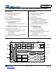
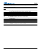
1. PIN DESCRIPTIONS
Pin Name # Pin Description
SDA 1 Serial Control Data (Input/Output) - Bidirectional data line for the I²C control port.
SCL 2 Serial Control Port Clock (Input) - Serial clock for the I²C control port.
VLC
3 Control Port Power (Input) - Determines the required signal level for the control port interface. Refer to
the Recommended Operating Conditions for appropriate voltages.
RESET
4 Reset (Input) - The device enters a low-power mode when this pin is driven low.
VA 5 Analog Power (Input) - Positive power for the internal analog section.
AGND 6 Analog Ground (Input) - Ground reference for the internal analog section.
AINA
AINB
7,
8
Analog Input (Input) - The full-scale level is specified in the ADC Analog Characteristics specification
table.
SGND 9 Signal Ground (Input) - Ground reference for the analog line inputs.
AFILTA
AFILTB
10,
11
Antialias Filter Connection (Output) - Antialias filter connection for the ADC inputs.
VQ 12 Quiescent Voltage (Output) - Filter connection for internal quiescent voltage.
FILT+ 13 Positive Voltage Reference (Output) - Positive reference voltage for the internal sampling circuits.
MICIN1
MICIN2
14,
15
Microphone Input (Input) - The full-scale level is specified in the ADC Analog Characteristics specifica-
tion table.
MICBIAS
16 Microphone Bias (Output) - Low noise bias supply for external microphone. Electrical characteristics
are specified in the DC Electrical Characteristics table.
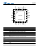
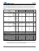
109
8
7
6
5
4
3
2
1
11
12
13 14 15 16
17
18
19
20
21
22
23
24
25
262728
29
303132
Top-Down (Through Package) View
32-Pin QFN Package
TXOUT
VD
DGND
MCLK
LRCK
SCLK
SDOUT
SDIN1
SGND
AFILTA
AFILTB
VQ
FILT+
MICIN1
MICIN2
MICBIAS
SDA
SCL
VLC
RESET
VA
AGND
AINA
AINB
SDIN2
TXSDIN
VLS
MUTEC
AOUTB
AOUTA
AGND
VA
Thermal Pad