CS4265 104 dB, 24-Bit, 192 kHz Stereo Audio CODEC D/A Features A/D Features Multi-Bit Delta Sigma Modulator Multi-Bit Delta Sigma Modulator 104 dB Dynamic Range 104 dB Dynamic Range -90 dB THD+N -95 dB THD+N Up to 192 kHz Sampling Rates Stereo 2:1 Input Multiplexer Single-Ended Analog Architecture Programmable Gain Amplifier (PGA) – – Volume Control with Soft Ramp – – 0.
CS4265 System Features Synchronous IEC60958-3 Transmitter – Up to 192 kHz Sampling Rates – 75 Drive Capability Serial Audio Data Input Multiplexer Internal Digital Loopback Supports Master or Slave Operation Mute Output Control Power-Down Mode – Available for A/D, D/A, CODEC, Mic Preamplifier +3.3 V to +5 V Analog Power Supply +3.3 V to +5 V Digital Power Supply Direct Interface with 1.
CS4265 TABLE OF CONTENTS 1. PIN DESCRIPTIONS .......................................................................................................................... 7 2. CHARACTERISTICS AND SPECIFICATIONS ...................................................................................... 9 SPECIFIED OPERATING CONDITIONS ............................................................................................. 9 ABSOLUTE MAXIMUM RATINGS ...............................................................
CS4265 6.3.1 DAC Digital Interface Format (Bits 5:4) ................................................................................. 37 6.3.2 Mute DAC (Bit 2) ................................................................................................................... 37 6.3.3 De-Emphasis Control (Bit 1) .................................................................................................. 38 6.4 ADC Control - Address 04h ..................................................................
CS4265 11.1.1 Accessing the E Buffer ........................................................................................................ 54 11.2 Serial Copy Management System (SCMS) .................................................................................. 54 11.3 Channel Status Data E Buffer Access .......................................................................................... 54 11.3.1 One-Byte Mode ...................................................................................
CS4265 Figure 42.Consumer Output Circuit (VD = 5 V) ........................................................................................ 52 Figure 43.TTL/CMOS Output Circuit ......................................................................................................... 52 Figure 44.Channel Status Data Buffer Structure ....................................................................................... 53 Figure 45.Flowchart for Writing the E Buffer ..........................................
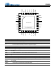
CS4265 TXOUT VD DGND MCLK LRCK SCLK SDOUT SDIN1 1.
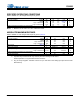
CS4265 VA 17 Analog Power (Input) - Positive power for the internal analog section. AGND 18 Analog Ground (Input) - Ground reference for the internal analog section. AOUTA AOUTB MUTEC VLS TXSDIN 19, 20 Analog Audio Output (Output) - The full scale output level is specified in the DAC Analog Characteristics specification table. 21 Mute Control (Output) - This pin is active during power-up initialization, reset, muting, when master clock left/right clock frequency ratio is incorrect, or power-down.
CS4265 2. CHARACTERISTICS AND SPECIFICATIONS SPECIFIED OPERATING CONDITIONS AGND = DGND = 0 V; All voltages with respect to ground. Parameters DC Power Supplies: Symbol Min Nom Max Units VA VD VLS VLC TA 3.13 3.13 1.71 1.71 -10 5.0 3.3 3.3 3.3 - 5.25 (Note 1) 5.25 5.25 +70 V V V V C Analog Digital Logic - Serial Port Logic - Control Port Ambient Operating Temperature (Power Applied) Notes: 1. Maximum of VA+0.25 V or 5.25 V, whichever is less.
CS4265 DAC ANALOG CHARACTERISTICS Test Conditions (unless otherwise specified): AGND = DGND = 0 V; VA = 3.13 V to 5.25 V; VD = 3.13 V to 5.25 V or VA + 0.25 V, whichever is less; VLS = VLC = 1.71 V to 5.25 V; TA = -10° to +70° C for Commercial or -40° to +85° C for Automotive; Output test signal: 997 Hz full-scale sine wave; Test load RL = 3 k, CL = 10 pF (see Figure 1), Fs = 48/96/192 kHz. Measurement Bandwidth 10 Hz to 20 kHz; All Connections as shown in Figure 9 on page 23.
CS4265 6. Guaranteed by design. See Figure 2. RL and CL reflect the recommended minimum resistance and maximum capacitance required for the internal op-amp’s stability. CL affects the dominant pole of the internal output amp; increasing CL beyond 100 pF can cause the internal op-amp to become unstable.
CS4265 3.3 µF V out AOUTx R L AGND C L Capacitive Load -- C L (pF) 125 100 75 25 2.5 3 Figure 1. DAC Output Test Load 12 Safe Operating Region 50 5 10 15 20 Resistive Load -- RL (k ) Figure 2.
CS4265 ADC ANALOG CHARACTERISTICS Test conditions (unless otherwise specified): AGND = DGND = 0 V; VA = 3.13 V to 5.25 V; VD = 3.13 V to 5.25 V or VA + 0.25 V, whichever is less; VLS = VLC = 1.71 V to 5.25 V; TA = -10° to +70° C for Commercial or -40° to +85° C for Automotive; Input test signal: 1 kHz sine wave; measurement bandwidth is 10 Hz to 20 kHz; Fs = 48/96/192 kHz.; All connections as shown in Figure 9 on page 23. Line-Level Inputs Parameter Dynamic Performance for VA = 4.75 V to 5.
CS4265 DC Accuracy Gain Error Gain Drift - 100 10 - % ppm/°C 0.51*VA 6.12 0.57*VA 6.8 0.63*VA 7.48 Vpp k - 5 - % Line-Level Input Characteristics Full-scale Input Voltage Input Impedance Maximum Interchannel Input Impedance Mismatch (Note 11) Line-Level and Microphone-Level Inputs Commercial Grade Parameter Symbol Min Typ Max Unit - 0.1 - dB - 0.5 - 0.4 dB dB DC Accuracy Interchannel Gain Mismatch Programmable Gain Characteristics Gain Step Size Absolute Gain Step Error 11.
CS4265 ADC ANALOG CHARACTERISTICS (Continued) Microphone-Level Inputs Parameter Dynamic Performance for VA = 4.75 V to 5.
CS4265 ADC DIGITAL FILTER CHARACTERISTICS Parameter (Notes 15, 17) Symbol Min Typ Max Unit 0 - 0.4896 Fs - - 0.035 dB 0.5688 - - Fs 70 - - dB - 12/Fs - s 0 - 0.4896 Fs - - 0.025 dB Single-Speed Mode Passband (-0.1 dB) Passband Ripple Stopband Stopband Attenuation Total Group Delay (Fs = Output Sample Rate) tgd Double-Speed Mode Passband (-0.1 dB) Passband Ripple Stopband Stopband Attenuation Total Group Delay (Fs = Output Sample Rate) tgd 0.
CS4265 DC ELECTRICAL CHARACTERISTICS AGND = DGND = 0 V, all voltages with respect to ground. MCLK=12.288 MHz; Fs=48 kHz; Master Mode. Parameter Symbol Min Typ Max Unit V V V V IA IA ID ID - 41 37 39 23 50 45 47 28 mA mA mA mA VA = 5 V VLS, VLC, VD=5 V IA ID - 0.50 0.54 - mA mA Power Consumption (Normal Operation) VA, VD, VLS, VLC = 5 V (Power-Down Mode) VA, VD, VLS, VLC = 3.3 V VA, VD, VLS, VLC = 5 V - - 400 198 4.2 485 241 - mW mW mW PSRR - 55 - dB VQ - 0.
CS4265 DIGITAL INTERFACE CHARACTERISTICS Test conditions (unless otherwise specified): AGND = DGND = 0 V; VLS = VLC = 1.71 V to 5.25 V. Parameters (Note 21) High-Level Input Voltage VL = 1.71 V VL > 2.
CS4265 SWITCHING CHARACTERISTICS - SERIAL AUDIO PORT Logic ‘0’ = DGND = AGND = 0 V; Logic ‘1’ = VL, CL = 20 pF. (Note 23) Parameter Sample Rate Single-Speed Mode Double-Speed Mode Quad-Speed Mode Symbol Min Typ Max Unit Fs Fs Fs 4 50 100 - 50 100 200 kHz kHz kHz fmclk tclkhl 1.024 8 45 50 51.
CS4265 LRCK O utput t slr SCLK O utput t sdo SDO UT t t sdis sdih SDIN Figure 3. Master Mode Serial Audio Port Timing LRCK Input t t sclkh slr t sclkl SCLK Input t t sdo sclkw SDOUT t sdis t sdih SDIN Figure 4.
CS4265 Channel B - Right Channel A - Left LRCK SCLK SDATA MSB -1 -2 -3 -4 -5 +5 +4 +3 +2 +1 LSB MSB -1 -2 -3 +5 -4 +4 +3 +2 +1 LSB Figure 5. Format 0, Left-Justified up to 24-Bit Data Channel A - Left LRCK Channel B - Right SCLK SDATA MSB -1 -2 -3 -4 -5 +5 +4 +3 +2 +1 LSB MSB -1 -2 -3 +5 +4 +3 +2 +1 LSB -4 Figure 6.
CS4265 SWITCHING CHARACTERISTICS - I²C CONTROL PORT Inputs: Logic 0 = DGND = AGND = 0 V, Logic 1 = VLC, CL = 30 pF. Parameter Symbol Min Max Unit SCL Clock Frequency fscl - 100 kHz RESET Rising Edge to Start tirs 500 - ns Bus Free Time Between Transmissions tbuf 4.7 - µs Start Condition Hold Time (prior to first clock pulse) thdst 4.0 - µs Clock Low time tlow 4.7 - µs Clock High Time thigh 4.0 - µs tsust 4.
CS4265 3. TYPICAL CONNECTION DIAGRAM +3.3V to +5V 10 µF 0.1 µF 0.1 µF VD +1.8V to +5V VA 0.1 µF VA Mute Drive MUTEC VLS 3.3 µF 47 k Note 4 SDIN1 AOUTB 3.3 µF TXSDIN Note 2 : C 10 k * C C TXOUT 10 µF 100 k * 1800 pF 100 k 10 µF SCL Signal Ground Right Analog Input 1 100 10 µF MICIN1 SDA Left Analog Input 1 * 1800 pF AIN1B RST 100 Microphone Input 1 Microphone Input 2 MICIN2 +1.8V to +5V 10 µF 2 k Note 1 RL VLC RL Note 3 MICBIAS 0.
CS4265 4. APPLICATIONS 4.1 Recommended Power-Up Sequence 1. Hold RESET low until the power supply, MCLK, and LRCK are stable. In this state, the Control Port is reset to its default settings. 2. Bring RESET high. The device will remain in a low power state with the PDN bit set by default. The control port will be accessible. 3. The desired register settings can be loaded while the PDN bit remains set. 4. Clear the PDN bit to initiate the power-up sequence. 4.
CS4265 In both Master and Slave Modes, the external MCLK must be divided down based on the MCLK/LRCK ratio to achieve a post-divider MCLK/LRCK ratio of 256x for SSM, 128x for DSM, or 64x for QSM. Table 3 lists the appropriate dividers. MCLK/LRCK Ratio MCLK Dividers 64x - - ÷1 96x - - ÷1.5 128x - ÷1 ÷2 192x - ÷1.5 ÷3 256x ÷1 ÷2 ÷4 384x ÷1.5 ÷3 - 512x ÷2 ÷4 - 768x ÷3 - - 1024x ÷4 - - Mode SSM DSM QSM Table 3. MCLK Dividers 4.2.
CS4265 which could result in recording a DC level, possibly yielding clicks when switching between devices in a multichannel system. The high-pass filter continuously subtracts a measure of the DC offset fro m the output of the decimation filter. If the HPFFreeze bit (See “ADC High-Pass Filter Freeze (Bit 1)” on page 39.) is set during normal operation, the current value of the DC offset for the each channel is frozen and this DC offset will continue to be subtracted from the conversion result.
CS4265 4.4 Analog Input Multiplexer, PGA, and Mic Gain The CS4265 contains a stereo 2-to-1 analog input multiplexer followed by a programmable gain amplifier (PGA). The input multiplexer is able to select either a line-level input source, or a mic-level input source, and route it to the PGA. The mic-level input passes through a +32 dB gain stage prior to the input multiplexer, allowing it to be used for microphone-level signals without the need for any external gain.
CS4265 topology. If pseudo-differential input functionality is not required, simply connect the SGND pin to AGND through the parallel combination of a 10 µF and a 0.1 µF capacitor. CS4265 A IN A VA + In to P G A 10 µF SGND 0.1 µF A IN B + - In to P G A N ote: If pseudo-differential input functionality is not required, the connections shown with dashed line should be added. Figure 12. Pseudo-Differential Input Stage 4.
CS4265 clocking change, the DAC outputs will always be in a zero-data state. If non-zero serial audio input is present at the time of switching, a slight click or pop may be heard as the DAC output automatically goes to its zero-data state. 4.8 DAC Serial Data Input Multiplexer The CS4265 contains a 2-to-1 serial data input multiplexer. This allows two se parate data sources to be input into the DAC without the use of any external multiplexing components. “Section 6.6.
CS4265 4.11 Mute Control The MUTEC pin becomes active during power-up initialization, reset, muting, if the MCLK to LRCK ratio is incorrect, and during power-down. The MUTEC pin is intended to be used as control for an external mute circuit in order to add off-chip mute capability. Use of the Mute Control function is not mandatory but recommended for designs requiring the absolute minimum in extraneous clicks and pops.
CS4265 under the control of a register bit. The CS4265 also allows immediate muting of the IEC60958-3 transmitter audio data through a control register bit. External components are used to terminate and isolate the external cable from the CS4265. These components are detailed in the “External IEC60958-3 Transmitter Components” section on page 52. 4.12.2 Mono Mode Operation An IEC60958-3 stream may be used in more than one way to transmit 192 kHz sample rate data.
CS4265 0 1 2 3 4 5 6 7 8 9 10 11 12 13 14 15 16 17 18 7 6 24 25 26 27 28 19 SCL CHIP ADDRESS (WRITE) 1 SDA 0 0 1 1 MAP BYTE 1 AD0 0 5 4 3 1 0 7 ACK 6 DATA +n DATA +1 DATA 2 1 ACK 0 7 6 1 0 7 6 1 0 ACK ACK STOP START Figure 15.
CS4265 4.15 Reset When RESET is low, the CS4265 enters a low-power mode and all internal states are reset, including the control port and registers, the outputs are muted. When RESET is high, the control port becomes operational, and the desired settings should be loaded into the control registers. Writing a 0 to the PDN bit in the Power Control register will then cause the part to leave the low-power state and begin operation.
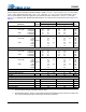
CS4265 5. REGISTER QUICK REFERENCE This table shows the register names and their associated default values.
CS4265 Addr Function 7 6 5 4 3 2 1 0 11h Transmitter Control 1 Reserved EFTCI CAM Reserved Reserved Reserved Reserved Reserved 0 0 0 0 0 0 0 0 12h Transmitter Control 2 Tx_DIF1 Tx_DIF0 TxOff TxMute V MMT MMTCS MMTLR 0 0 0 0 0 0 0 0 - - - - - - - - 13h - C-Data Buffer 2Ah DS657F3 35
CS4265 6. REGISTER DESCRIPTION 6.1 Chip ID - Register 01h 7 PART3 6 PART2 5 PART1 4 PART0 3 REV3 2 REV2 1 REV1 0 REV0 Function: This register is Read-Only. Bits 7 through 4 are the part number ID, which is 1101b (0Dh), and the remaining bits (3 through 0) indicate the device revision as shown in Table 5 below. REV[2:0] Revision 001 A 010 B, C0 011 C1 Table 5. Device Revision 6.2 Power Control - Address 02h 7 Freeze 6.2.
CS4265 6.2.4 Power-Down DAC (Bit 1) Function: The DAC pair will remain in a reset state whenever this bit is set. 6.2.5 Power-Down Device (Bit 0) Function: The device will enter a low-power state whenever this bit is set. The power-down bit is set by default and must be cleared before normal operation can occur. The contents of the control registers are retained when the device is in power-down. 6.
CS4265 6.3.3 De-Emphasis Control (Bit 1) Function: The standard 50/15 s digital de-emphasis filter response, Figure 17, may be implemented for a sample rate of 44.1 kHz when the DeEmph bit is configured as shown in Table 8. NOTE: De-emphasis is available only in Single-Speed Mode. DeEmph 0 1 Description Disabled (default) 44.1 kHz de-emphasis Table 8. De-Emphasis Control Gain dB T1=50 µs 0dB T2 = 15 µs -10dB F1 3.183 kHz F2 Frequency 10.61 kHz Figure 17. De-Emphasis Curve 6.
CS4265 ADC_DIF Description Format Figure 0 Left-Justified, up to 24-bit data (default) 0 5 1 I²S, up to 24-bit data 1 6 Table 10. ADC Digital Interface Formats 6.4.3 Mute ADC (Bit 2) Function: When this bit is set, the serial audio output of the both ADC channels is muted. 6.4.4 ADC High-Pass Filter Freeze (Bit 1) Function: When this bit is set, the internal high-pass filter is disabled. The current DC offset value will be frozen and continue to be subtracted from the conversion result.
CS4265 6.6 Signal Selection - Address 06h 7 6 5 4 3 2 1 0 SDINSel Reserved Reserved Reserved Reserved Reserved LOOP Reserved 6.6.1 DAC SDIN Source (Bit 7) Function: This bit is used to select the serial audio data source for the DAC as shown in Table 12. SDINSel Setting DAC Data Source 0 1 SDIN1 SDIN2 Table 12. DAC SDIN Source Selection 6.6.2 Digital Loopback (Bit 1) Function: When this bit is set, an internal digital loopback from the ADC to the DAC will be enabled.
CS4265 6.9 ADC Input Control - Address 09h 7 Reserved 6.9.1 6 Reserved 5 Reserved 4 PGASoft 3 PGAZero 2 Reserved 1 Reserved 0 Select PGA Soft Ramp or Zero Cross Enable (Bits 4:3) Function: Soft Ramp Enable Soft Ramp allows level changes, both muting and attenuation, to be implemented by incrementally ramping, in 1/8 dB steps, from the current level to the new level at a rate of 1 dB per 8 left/right clock periods. See Table 14.
CS4265 6.11 DAC Channel B Volume Control - Address 0Bh 7 Vol7 6.11.1 6 Vol6 5 Vol5 4 Vol4 3 Vol3 2 Vol2 1 Vol1 0 Vol0 Volume Control (Bits 7:0) Function: The digital volume control allows the user to attenuate the signal in 0.5 dB increments from 0 to -127 dB. The Vol0 bit activates a 0.5 dB attenuation when set, and no attenuation when cleared. The Vol[7:1] bits activate attenuation equal to their decimal equivalent (in dB). Example volume settings are decoded as shown in Table 16.
CS4265 ple rate) if the signal does not encounter a zero crossing. The zero cross function is independently monitored and implemented for each channel. See Table 17. DACSoft DACZeroCross Mode 0 0 Changes to affect immediately 0 1 Zero Cross enabled 1 0 Soft Ramp enabled 1 1 Soft Ramp and Zero Cross enabled (default) Table 17. DAC Soft Cross or Zero Cross Mode Selection 6.12.2 Invert DAC Output (Bit 5) Function: When this bit is set, the output of the DAC is inverted. 6.
CS4265 6.14 Status Mask - Address 0Eh 7 Reserved 6 Reserved 5 Reserved 4 EFTCM 3 ClkErrM 2 Reserved 1 ADCOvflM 0 ADCUndrflM Function: The bits of this register serve as a mask for the Status sources found in the register “Status - Address 0Dh” on page 43. If a mask bit is set to 1, the error is unmasked, meaning that its occurrence will affect the status register. If a mask bit is set to 0, the error is masked, meaning that its occurrence will not affect the status register.
CS4265 6.18 Transmitter Control 2 - Address 12h 7 Tx_DIF1 6 Tx_DIF0 5 TxOff 4 TxMute 3 V 2 MMT 1 MMTCS 0 MMTLR 6.18.1 Transmitter Digital Interface Format (Bits 7:6) Function: The required relationship between LRCK, SCLK and SDIN for the transmitter is defined by the Transmitter Digital Interface Format and the options are detailed in Table 18 and Figures 5-7.
CS4265 6.18.7 Mono Mode Channel Selection (Bit 0) Function: When this bit is cleared, channel A input data will be transmitted in both channel A and B subframes in mono mode. When this bit is set, channel B input data will be transmitted in both channel A and B subframes in Mono Mode.
CS4265 7. PARAMETER DEFINITIONS Dynamic Range The ratio of the rms value of the signal to the rms sum of all other spectral components over the specified bandwidth. Dynamic Range is a signal-to-noise ratio measurement over the specified bandwidth made with a -60 dBFS signal. 60 dB is added to resulting measurement to refer the measurement to full scale. This technique ensures that the distortion components are below the noise level and do not affect the measurement.
CS4265 8. DAC FILTER PLOTS Figure 18. DAC Single-Speed Stopband Rejection Figure 19. DAC Single-Speed Transition Band 0 -1 0.05 -2 0 -3 -0.05 Amplitude dB Amplitude dB -4 -5 -6 -0. 1 -0.15 -7 -0. 2 -8 -0.25 -9 -10 0.45 48 0.46 0.47 0.48 0.49 0.5 0.51 Frequency (normalized to Fs) 0.52 0.53 0.54 0.5 5 0 0.05 0.1 0.15 0.2 0.25 0.3 Frequency (normalized to Fs) 0.35 0.4 0.45 Figure 20. DAC Single-Speed Transition Band Figure 21. DAC Single-Speed Passband Ripple Figure 22.
CS4265 1 0.8 0 0.7 -1 0.6 -2 0.5 Amplitude dB Amplitude dB -3 -4 -5 0.4 0.3 0.2 -6 0.1 -7 0 -8 -0. 1 -9 - 10 0.45 0.46 0.47 0.48 0.49 0.5 0.51 Frequency (normalized to Fs) 0.52 0.53 0.54 -0. 2 0.55 0 Figure 24. DAC Double-Speed Transition Band 0.05 0.1 0.15 0.2 0.25 0.3 Frequency (normalized to Fs) 0.35 0.4 0.45 0.5 Figure 25.
CS4265 0 -10 -20 -30 -40 -50 -60 -70 -80 -90 -100 -110 -120 -130 -140 Amplitude (dB) Amplitude (dB) 9. ADC FILTER PLOTS 0.0 0.1 0.2 0.3 0.4 0.5 0.6 0.7 0.8 0.9 1.0 0 -10 -20 -30 -40 -50 -60 -70 -80 -90 -100 -110 -120 -130 -140 0.40 0.42 0.44 Frequency (norm alized to Fs) 0 0.10 -1 0.08 -2 0.06 -3 0.04 -4 -5 -6 -7 0.58 0.60 0.00 -0.04 -0.06 -0.08 -0.10 0.46 0.47 0.48 0.49 0.5 0.51 0.52 0.53 0.54 0 0.55 0.2 0.3 0.4 0.5 0.6 0.7 0.8 0.1 0.15 0.2 0.25 0.3 0.
0 0.10 -1 0.08 -2 0.06 -3 0.04 Amplitude (dB) Amplitude (dB) CS4265 -4 -5 -6 -7 0.02 0.00 -0.02 -0.04 -8 -0.06 -9 -0.08 -10 0.46 0.47 0.48 0.49 0.50 0.51 -0.10 0.00 0.05 0.52 Frequency (norm alized to Fs) 0 -10 -20 -30 -40 -50 -60 -70 -80 -90 -100 -110 -120 -130 -140 0.1 0.2 0.3 0.4 0.5 0.6 0.7 0.8 0.15 0.20 0.25 0.30 0.35 0.40 0.45 0.50 Figure 37. ADC Double-Speed Passband Ripple Amplitude (dB) Amplitude (dB) Figure 36. ADC Double-Speed Transition Band (Detail) 0.
CS4265 10.EXTERNAL IEC60958-3 TRANSMITTER COMPONENTS This section details the external components required to interface the IEC60958-3 transmitter to cables and fiberoptic components. 10.1 IEC60958-3 Transmitter External Components The IEC60958-3 specifications call for an unbalanced drive circuit with an output impedance of 75 and an output drive level of 0.5 volts peak-to-peak ±20% when measured across a 75 load using no cable.
CS4265 11.CHANNEL STATUS BUFFER MANAGEMENT The CS4265 has a comprehensive channel status (C) data buffering scheme which allows the user to manage the C data through the control port. 11.1 IEC60958-3 Channel Status (C) Bit Management The CS4265 contains sufficient RAM to store a full block of C data for both A and B channels (192x2 = 384 bits). The user may read from, or write to, these RAM buffers through the control port.
CS4265 11.1.1 Accessing the E Buffer The user can monitor the data being transferred by reading the E buffer, which is mapped into the register space of the CS4265, through the control port. The user can modify the data to be transmitted by writing to the E buffer. The E buffer is only accessible when an MCLK signal is applied to the CS4265 and the device is out of the power-down state (the PDN bit in register 02h is cleared).
CS4265 11.3.1 One-Byte Mode In many applications, the channel status blocks for the A and B channels will be identical. In this situation, if the user reads a byte from one of the channel's blocks, the corresponding byte for the other channel will be the same. Similarly, if the user wrote a byte to one channel's block, it would be necessary to write the same byte to the other block. One-Byte Mode takes advantage of the often identical nature of A and B channel status data.
CS4265 12.PACKAGE DIMENSIONS 32L QFN (5 X 5 mm BODY) PACKAGE DRAWING e b D Pin #1 Corner Pin #1 Corner E2 E A1 L A Top View DIM A A1 b D D2 E E2 e L 0.1280 0.1280 0.0118 Bottom View Side View INCHES NOM --0.0091 0.1969 BSC 0.1299 0.1969 BSC 0.1299 0.0197 BSC 0.0157 MIN -0.0000 0.0071 D2 MAX 0.0394 0.0020 0.0110 MIN -0.00 0.18 0.1319 3.25 0.1319 3.25 0.0197 0.30 MILLIMETERS NOM --0.23 5.00 BSC 3.30 5.00 BSC 3.30 0.50 BSC 0.40 NOTE MAX 1.00 0.05 0.28 3.35 3.35 0.
CS4265 14.ORDERING INFORMATION Product CS4265 CS4265 CDB4265 Description 24-bit, 192 kHz Stereo Audio CODEC 24-bit, 192 kHz Stereo Audio CODEC Package Pb-Free 32-QFN 32-QFN CS4265 Evaluation Board Yes Grade Commercial Temp Range -10° to +70° C Yes Automotive -40° to +105° C No - - Container Order # Tube CS4265-CNZ Tape & Reel CS4265-CNZR Tube CS4265-DNZ Tape & Reel CS4265-DNZR - CDB4265 15.