CS42518 110 dB, 192-kHz 8-Ch CODEC with S/PDIF Receiver Features General Description Eight 24-bit D/A, two 24-bit A/D Converters The CS42518 provides two analog-to-digital and eight digital-to-analog delta-sigma converters, as well as an integrated S/PDIF receiver. 110 dB DAC / 114 dB ADC Dynamic Range -100 dB THD+N The CS42518 integrated S/PDIF receiver supports up to eight inputs, clock recovery circuitry and format autodetection.
CS42518 TABLE OF CONTENTS 1. CHARACTERISTICS AND SPECIFICATIONS ...................................................................................... 6 SPECIFIED OPERATING CONDITIONS ............................................................................................... 6 ABSOLUTE MAXIMUM RATINGS ......................................................................................................... 6 ANALOG INPUT CHARACTERISTICS ....................................................................
CS42518 6. REGISTER DESCRIPTION .................................................................................................................. 45 6.1 Memory Address Pointer (MAP) ..................................................................................................... 45 6.2 Chip I.D. and Revision Register (address 01h) (Read Only) .......................................................... 45 6.3 Power Control (address 02h) ....................................................................
CS42518 10.1.4 Circuit Board Layout ............................................................................................................ 81 11. APPENDIX D: EXTERNAL AES3-S/PDIF-IEC60958 RECEIVER COMPONENTS .......................... 82 11.1 AES3 Receiver External Components .......................................................................................... 82 12. APPENDIX E: ADC FILTER PLOTS ..................................................................................................
CS42518 Figure 42. Quad-Speed Mode Stopband Rejection .................................................................................. 84 Figure 43. Quad-Speed Mode Transition Band ........................................................................................ 84 Figure 44. Quad-Speed Mode Transition Band (Detail) ............................................................................ 84 Figure 45. Quad-Speed Mode Passband Ripple ..............................................................
CS42518 1. CHARACTERISTICS AND SPECIFICATIONS (All Min/Max characteristics and specifications are guaranteed over the Specified Operating Conditions. Typical performance characteristics and specifications are derived from measurements taken at nominal supply voltages and TA = 25° C.) SPECIFIED OPERATING CONDITIONS (AGND=DGND=0, all voltages with respect to ground; OMCK=12.
CS42518 ANALOG INPUT CHARACTERISTICS (TA = 25° C; VA =VARX= 5 V, VD = 3.3 V, Logic “0” = DGND =AGND = 0 V; Logic “1” = VLS = VLC = 5 V; Measurement Bandwidth is 10 Hz to 20 kHz unless otherwise specified. Full-scale input sine wave, 997 Hz.; PDN_RCVR = 1; SW_CTRL[1:0] = ‘01’; OMCK = 12.288 MHz; Single-Speed Mode CX_SCLK = 3.072 MHz; Double-Speed Mode CX_SCLK = 6.144 MHz; Quad-Speed Mode CX_SCLK = 12.288 MHz.
CS42518 A/D DIGITAL FILTER CHARACTERISTICS Parameter Symbol Min Typ Max Unit (Note 5) 0 - 0.47 Fs - - 0.035 dB (Note 5) 0.58 - - Fs Single-Speed Mode (2 to 50 kHz sample rates) Passband (-0.1 dB) Passband Ripple Stopband Stopband Attenuation -95 - - dB tgd - 12/Fs - s tgd - - 0.0 s (Note 5) 0 - 0.45 Fs - - 0.035 dB (Note 5) 0.68 - - Fs Total Group Delay (Fs = Output Sample Rate) Group Delay Variation vs.
CS42518 ANALOG OUTPUT CHARACTERISTICS (TA = 25° C; VA =VARX= 5 V, VD = 3.3 V, Logic “0” = DGND =AGND = 0 V; Logic “1” = VLS = VLC = 5V; Measurement Bandwidth 10 Hz to 20 kHz unless otherwise specified.; Full-scale output 997 Hz sine wave, Test load RL = 3 k, CL = 30 pF; PDN_RCVR = 1; SW_CTRL[1:0] = ‘01’; OMCK = 12.288 MHz; Single-Speed Mode, CX_SCLK = 3.072 MHz; Double-Speed Mode, CX_SCLK = 6.144 MHz; Quad-Speed Mode, CX_SCLK = 12.288 MHz.
CS42518 D/A DIGITAL FILTER CHARACTERISTICS Fast Roll-Off Slow Roll-Off Parameter Min Typ Max Min Typ Max Combined Digital and On-chip Analog Filter Response - Single-Speed Mode - 48 kHz Passband (Note 9) to -0.01 dB corner 0 to -3 dB corner 0 Frequency Response 10 Hz to 20 kHz -0.01 StopBand 0.5465 StopBand Attenuation (Note 10) 90 Group Delay Passband Group Delay Deviation 0 - 20 kHz De-emphasis Error (Note 11) Fs = 32 kHz (Relative to 1 kHz) Fs = 44.1 kHz Fs = 48 kHz - 12/Fs - 0.4535 0.4998 +0.01 ±0.
CS42518 SWITCHING CHARACTERISTICS (TA = -10 to +70° C; VA=VARX = 5 V, VD =VLC= 3.3 V, VLS = 1.8 V to 5.25 V; Inputs: Logic 0 = DGND, Logic 1 = VLS, CL = 30 pF) Parameters Symbol RST Pin Low Pulse Width (Note 12) PLL Clock Recovery Sample Rate Range Min Typ Max Units 1 - - ms 30 - 200 kHz - 200 - ps RMS RMCK Output Jitter (Note 14) RMCK Output Duty Cycle (Note 15) 45 50 55 % OMCK Frequency (Note 13) 1.024 - 25.
CS42518 SWITCHING CHARACTERISTICS - CONTROL PORT - I²C™ FORMAT (TA = -10 to +70° C; VA=VARX = 5 V, VD =VLS= 3.3 V; VLC = 1.8 V to 5.25 V; Inputs: Logic 0 = DGND, Logic 1 = VLC, CL = 30 pF) Parameter Symbol Min Max Unit SCL Clock Frequency fscl - 100 kHz RST Rising Edge to Start tirs 500 - ns Bus Free Time Between Transmissions tbuf 4.7 - µs Start Condition Hold Time (prior to first clock pulse) thdst 4.0 - µs Clock Low time tlow 4.7 - µs Clock High Time thigh 4.
CS42518 SWITCHING CHARACTERISTICS - CONTROL PORT - SPI™ FORMAT (TA = -10 to +70° C; VA=VARX = 5 V, VD =VLS= 3.3 V; VLC = 1.8 V to 5.25 V; Inputs: Logic 0 = DGND, Logic 1 = VLC, CL = 30 pF) Parameter Symbol Min Typ Max Units fsck 0 - 6.0 MHz CS High Time Between Transmissions tcsh 1.
CS42518 DC ELECTRICAL CHARACTERISTICS (TA = 25° C; AGND=DGND=0, all voltages with respect to ground; OMCK=12.288 MHz; Master Mode) Parameter Symbol Min Typ Max Units IA ID ID ILC ILS Ipd - 75 85 51 250 13 250 - mA mA mA A mA A - 587 1.25 866 1.25 650 960 - mW mW mW mW - 60 40 - dB dB VQ Nominal Voltage VQ Output Impedance VQ Maximum allowable DC current - 2.7 50 0.01 - V k mA FILT+ Nominal Voltage FILT+ Output Impedance FILT+ Maximum allowable DC current - 5.0 35 0.
CS42518 DIGITAL INTERFACE CHARACTERISTICS (TA = +25° C) Parameters (Note 27) High-Level Input Voltage Low-Level Input Voltage High-Level Output Voltage at Io=2 mA Low-Level Output Voltage at Io=2 mA Serial Port, Control Port, MUTEC, GPOx,TXP High-Level Output Voltage at Io=100 A Low-Level Output Voltage at Io=100 A Input Sensitivity, RXP[7:0] Input Leakage Current Input Capacitance MUTEC Drive Current Serial Port Control Port Serial Port Control Port (Note 28)Serial Port Control Port MUTEC, GPOx TXP (
CS42518 TXP RXP0 VD VLS DGND SAI_SDOUT RM CK CX_SDOUT ADCIN2 ADCIN1 OMCK SAI_LRCK CX_SDIN4 SAI_SCLK CX_SDIN2 CX_SDIN3 2.
CS42518 Interrupt (Output) - The CS42518 will generate an interrupt condition as per the Interrupt Mask register. See “Interrupts” on page 39 for more details. INT 11 RST 12 AINRAINR+ 13 14 Reset (Input) - The device enters a low power mode and all internal registers are reset to their default settings when low. Differential Right Channel Analog Input (Input) - Signals are presented differentially to the delta-sigma modulators via the AINR+/- pins.
CS42518 OMCK 59 SAI_LRCK 60 SAI_SCLK 61 18 External Reference Clock (Input) - External clock reference that must be within the ranges specified in the register “OMCK Frequency (OMCK Freqx)” on page 52. Serial Audio Interface Left/Right Clock (Input/Output) - Determines which channel, Left or Right, is currently active on the serial audio data line. Serial Audio Interface Serial Clock (Input/Output) - Serial clock for the Serial Audio Interface.
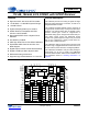
CS42518 3. TYPICAL CONNECTION DIAGRAM + 3.3 V to + 5 V 10 µ F 10 µ F + 0.1 µ F 0.01 µ F 0.01 µ F 0.1 µ F + + 0.1 µ F 0.01 µ F 0.01 µ F 0.1 µ F + 51 4 VD 50 D river 49 S /P D IF Interfac e 48 47 46 U p to 8 S ources 45 44 43 42 +2.5 V to + 5 V 53 0.1 µ F 59 OSC 58 C S 5361 A /D C onverter C S 5361 A /D C onv erter 57 55 54 60 61 D igital A udio P rocessor 3 2 56 1 64 63 62 11 12 M ic roC ontroller 7 8 9 10 ** 2 k +1.
CS42518 4. APPLICATIONS 4.1 Overview The CS42518 is a highly integrated mixed-signal 24-bit audio codec comprised of 2 analog-to-digital converters (ADC), implemented using multi-bit delta-sigma techniques, 8 digital-to-analog converters (DAC) and a 192 kHz digital audio S/PDIF receiver.
CS42518 4.2.2 High-Pass Filter and DC Offset Calibration The high-pass filter continuously subtracts a measure of the DC offset from the output of the decimation filter. The high-pass filter can be independently enabled and disabled. If the HPF_Freeze bit is set during normal operation, the current value of the DC offset for the corresponding channel is frozen and this DC offset will continue to be subtracted from the conversion result.
CS42518 4.3.3 Digital Volume and Mute Control Each DAC’s output level is controlled via the Volume Control registers operating over the range of 0 to -127 dB attenuation with 0.5 dB resolution. See “Volume Control (addresses 0Fh, 10h, 11h, 12h, 13h, 14h, 15h, 16h)” on page 58. Volume control changes are programmable to ramp in increments of 0.125 dB at the rate controlled by the SZC[1:0] bits in the Digital Volume Control register. See “Volume Transition Control (address 0Dh)” on page 56.
CS42518 4.4 S/PDIF Receiver The CS42518 includes an S/PDIF digital audio receiver. The S/PDIF receiver accepts and decodes digital audio data according to the IEC60958 (S/PDIF), and EIAJ CP-1201 interface standards. The receiver consists of an 8:2 multiplexer input stage driven through pins RXP0 and RXP1/GPO1 - RXP7/GPO7, a PLL based clock recovery circuit, and a decoder which separates the audio data from the channel status and user data.
CS42518 4.5 Clock Generation The clock generation for the CS42518 is shown in the figure below. The internal MCLK is derived from the output of the PLL or a master clock source attached to OMCK. The mux selection is controlled by the SW_CTRLx bits and can be configured to manual switch mode only, or automatically switch on loss of PLL lock to the other source input. RMCK_DIVx bits 2 4 Internal MCLK Recovered S/PDIF Clock SAI_LRCK (slave mode) 0 1 PLL (256Fs) 8.192 49.
CS42518 4.5.2 OMCK System Clock Mode A special clock-switching mode is available that allows the clock that is input through the OMCK pin to be used as the internal master clock. This feature is controlled by the SW_CTRLx bits in register “Clock Control (address 06h)” on page 52. An advanced auto-switching mode is also implemented to maintain master clock functionality.
CS42518 When either serial port is in Slave Mode, its respective LRCK signal must be present for proper device operation. In Slave Mode, One-Line Mode #1 is supported; One-Line Mode #2 is not. The sample rate to OMCK ratios and OMCK frequency requirements for Slave Mode operation are shown in Table 1. Refer to Table 3 for required clock ratios.
CS42518 Serial Inputs / Outputs CX_SDIN1 left channel DAC #1 right channel DAC #2 One-Line Mode DAC channels 1,2,3,4,5,6 CX_SDIN2 left channel DAC #3 right channel DAC #4 One-Line Mode not used CX_SDIN3 left channel DAC #5 right channel DAC #6 One-Line Mode not used CX_SDIN4 left channel DAC #7 right channel DAC #8 One-Line Mode DAC channels 7,8 CX_SDOUT left channel ADC #1 right channel ADC #2 One-Line Mode ADC channels 1,2,3,4,5,6 SAI_SDOUT left channel S/PDIF Left or ADC #1 right channel S/PDI
CS42518 4.6.2 Serial Audio Interface Formats The CODEC_SP and SAI_SP digital audio serial ports support five formats with varying bit depths from 16 to 24 as shown in Figures 10 to 14. These formats are selected using the configuration bits in the registers, “Functional Mode (address 03h)” on page 47 and “Interface Formats (address 04h)” on page 49. For the diagrams below, Single-Speed Mode is equivalent to Fs = 32, 44.1, 48 kHz; Double-Speed Mode is for Fs = 64, 88.
CS42518 CX_LRCK SAI_LRCK Left Channel Right Channel CX_SCLK SAI_SCLK CX_SDINx CX_SDOUT SAI_SDOUT MSB -1 -2 -3 -4 -5 +5 +4 +3 +2 +1 LSB MSB -1 -2 -3 -4 +5 +4 +3 +2 +1 LSB Left-Justified Mode, Data Valid on Rising Edge of SCLK SCLK Rate(s) Bits/Sample 16 18 to 24 Master Notes Slave 64 32, 48, 64, 128 Fs Single-Speed Mode 64 Fs 32, 64 Fs Double-Speed Mode 64 Fs 32, 64 Fs Quad-Speed Mode 64, 128, 256 Fs 48, 64, 128 Fs Single-Speed Mode 64 Fs 48, 64 Fs Double-Speed Mode 64 Fs
CS42518 CX_LRCK SAI_LRCK CX_SCLK SAI_SCLK CX_SDIN1 MSB CX_SDIN4 CX_SDOUT SAI_SDOUT 64 clks 64 clks Left Channel Right Channel LSB MSB LSB MSB LSB MSB LSB MSB LSB MSB DAC1 DAC3 DAC5 DAC2 DAC4 DAC6 20 clks 20 clks 20 clks 20 clks 20 clks 20 clks DAC7 DAC8 20 clks 20 clks ADC1 ADC3 ADC5 ADC2 ADC4 ADC6 20 clks 20 clks 20 clks 20 clks 20 clks 20 clks LSB MSB LSB MSB One-Line Data Mode #1, Data Valid on Rising Edge of SCLK SCLK Rate(s) Bits/Sample 20 Master Notes
CS42518 4.6.3 ADCIN1/ADCIN2 Serial Data Format The two serial data lines which interface to the optional external ADCs, ADCIN1 and ADCIN2, support only left-justified, 24-bit samples at 64Fs or 128Fs. This interface is not affected by any of the serial port configuration register bit settings. These serial data lines are used when supporting One-Line Mode of operation with external ADCs attached. If these signals are not being used, they should be tied together and wired to GND via a pull-down resistor.
CS42518 4.6.4 One-Line Mode (OLM) Configurations 4.6.4.1 OLM Config #1 One-Line Mode Configuration #1 can support up to 8 channels of DAC data, 6 channels of ADC data and 2 channels of S/PDIF received data. This is the only configuration which will support up to 24-bit samples at a sampling frequency of 48 kHz on all channels for both the DAC and ADC.
CS42518 4.6.4.2 OLM Config #2 This configuration will support up to 8 channels of DAC data or 6 channels of ADC data and no channels of S/PDIF received data and will handle up to 20-bit samples at a sampling-frequency of 96 kHz on all channels for both the DAC and ADC. The output data stream of the internal and external ADCs is configured to use the SAI_SDOUT output and run at the SAI_SP clock speeds.
CS42518 4.6.4.3 OLM Config #3 This One Line Mode configuration #3 will support up to 8 channels of DAC data, 6 channels of ADC data and 2 channels of S/PDIF received data and will handle up to 20-bit samples at a sampling frequency of 48 kHz on all channels for both the DAC and ADC. The output data stream of the internal and external ADCs is configured to use the CX_SDOUT output and run at the CODEC_SP clock speeds. One Line Mode #2, which supports 24-bit samples, is not supported by this configuration.
CS42518 4.6.4.4 OLM Config #4 This configuration will support up to 8 channels of DAC data 6 channels of ADC data and no channels of S/PDIF received data. OLM Config #4 will handle up to 20-bit ADC samples at an Fs of 48 kHz and 24bit DAC samples at an Fs of 48 kHz.
CS42518 4.6.4.5 OLM Config #5 This One-Line Mode configuration can support up to 8 channels of DAC data 2 channels of ADC data and 2 channels of S/PDIF received data and will handle up to 24-bit samples at a sampling frequency of 48 kHz on all channels for both the DAC and ADC. The output data stream of the internal ADCs can be configured to use the CX_SDOUT output and run at the CODEC_SP clock speeds or to use the SAI_SDOUT data output and run at the SAI_SP rate.
CS42518 4.7 Control Port Description and Timing The control port is used to access the registers, allowing the CS42518 to be configured for the desired operational modes and formats. The operation of the control port may be completely asynchronous with respect to the audio sample rates. However, to avoid potential interference problems, the control port pins should remain static if no operation is required. The control port has two modes: SPI and I²C, with the CS42518 acting as a slave device.
CS42518 4.7.2 I²C Mode In I²C mode, SDA is a bidirectional data line. Data is clocked into and out of the part by the clock, SCL. There is no CS pin. Pins AD0 and AD1 form the two least-significant bits of the chip address and should be connected through a resistor to VLC or DGND as desired. The state of the pins is sensed while the CS42518 is being reset. The signal timings for a read and write cycle are shown in Figure 22 and Figure 23.
CS42518 Send start condition. Send 10011xx1(chip address & read operation). Receive acknowledge bit. Receive byte, contents of selected register. Send acknowledge bit. Send stop condition. Setting the auto increment bit in the MAP allows successive reads or writes of consecutive registers. Each byte is separated by an acknowledge bit. 4.8 Interrupts The CS42518 has a comprehensive interrupt capability. The INT output pin is intended to drive the interrupt input pin on the host microcontroller.
CS42518 For applications where the output of the PLL is required to be low jitter, use a separate, low-noise analog +5 V supply for VARX, decoupled to AGND. In addition, a separate region of analog ground plane around the FILT+, VQ, LPFLT, REFGND, AGND, VA, VARX, RXP/and RXP0 pins is recommended. Extensive use of power and ground planes, ground plane fill in unused areas and surface mount decoupling capacitors are recommended. Decoupling capacitors should be as near to the pins of the CS42518 as possible.
CS42518 5.
CS42518 Addr Function 0Fh 10h 11h 12h 13h 14h 15h 16h 17h 18h 19h 1Ah 1Bh 1Ch 1Dh 42 Vol. Control A1 page 58 default Vol. Control B1 page 58 default Vol. Control A2 page 58 default Vol. Control B2 page 58 default Vol. Control A3 page 58 default Vol. Control B3 page 58 default Vol. Control A4 page 58 default Vol.
CS42518 Addr Function 1Eh 1Fh 20h 21h 22h 23h 24h 25h 26h 27h 28h 29h 2Ah 2Bh 2Ch RCVR Mode Ctrl page 61 default RCVR Mode Ctrl 2 page 63 default Interrupt Status page 63 default Interrupt Mask page 64 default Interrupt Mode MSB page 65 default Interrupt Mode LSB page 65 default Buffer Ctrl page 65 default RCVR CS Data. page 66.
CS42518 Addr Function 7 6 5 4 3 2 1 0 RXP3/GPO 3 page 69 default 2Eh RXP2/GPO 2 page 69 default 2Fh RXP1/GPO 1 page 69 default 30h Q Subcode page 71 default 31h Q Subcode page 71 default 32h Q Subcode page 71 default 33h Q Subcode page 71 default 34h Q Subcode page 71 default 35h Q Subcode page 71 default 36h Q Subcode page 71 default 37h Q Subcode page 71 default 38h Q Subcode page 71 default 39h Q Subcode page 71 default 3Ah - C or U Data Buffer 51h page 71 default Mode1 Mode0 Polarity Functi
CS42518 6. REGISTER DESCRIPTION All registers are read/write except for the I.D. and Revision Register, OMCK/PLL_CLK Ratio Register, Interrupt Status Register, and Q-Channel Subcode Bytes and C-bit or U-bit Data Buffer, which are read only. See the following bit definition tables for bit assignment information. The default state of each bit after a power-up sequence or reset is listed in each bit description. 6.1 Memory Address Pointer (MAP) Not a register 7 INCR 6.1.
CS42518 6.3 Power Control (address 02h) 7 6 PDN_RCVR1 PDN_RCVR0 6.3.1 5 PDN_ADC 4 PDN_DAC4 3 PDN_DAC3 2 PDN_DAC2 1 PDN_DAC1 0 PDN POWER DOWN RECEIVER (PDN_RCVRX) Default = 10 00 - Receiver and PLL in normal operational mode. 01 - Receiver and PLL held in a reset state. Equivalent to setting 11. 10 - Reserved. 11 - Receiver and PLL held in a reset state. Equivalent to setting 01. Function: Places the S/PDIF receiver and PLL in a reset state.
CS42518 6.4 Functional Mode (address 03h) 7 6 CODEC_FM1 CODEC_FM0 6.4.1 5 SAI_FM1 4 SAI_FM0 3 2 ADC_SP SEL1 ADC_SP SEL0 1 DAC_DEM 0 RCVR_DEM CODEC FUNCTIONAL MODE (CODEC_FMX) Default = 00 00 - Single-Speed Mode (4 to 50 kHz sample rates) 01 - Double-Speed Mode (50 to 100 kHz sample rates) 10 - Quad-Speed Mode (100 to 192 kHz sample rates) 11 - Reserved Function: Selects the required range of sample rates for all converters clocked from the Codec serial port (CODEC_SP).
CS42518 Receiver Mode Control (address 1Eh) register to set the appropriate sample rate. DAC_DEM reg03h[1] FRC_PLL_LK reg06h[0] DE-EMPH[1:0] reg1Eh[5:4] De-Emphasis Mode 0 1 1 X 0 1 XX XX 00 01 10 11 No De-Emphasis Auto-Detect Fs Reserved 32 kHz 44.1 kHz 48 kHz Table 5. DAC De-Emphasis 6.4.5 RECEIVER DE-EMPHASIS CONTROL (RCVR_DEM) Default = 0 Function: When enabled, de-emphasis will be automatically applied when emphasis is detected based on the channel status bits.
CS42518 6.5 Interface Formats (address 04h) 7 DIF1 6.5.1 6 DIF0 5 ADC_OL1 4 ADC_OL0 3 DAC_OL1 2 DAC_OL0 1 SAI_RJ16 0 CODEC_RJ16 DIGITAL INTERFACE FORMAT (DIFX) Default = 01 Function: These bits select the digital interface format used for the CODEC Serial Port and Serial Audio Interface Port when not in One-Line Mode. The required relationship between the Left/Right clock, serial clock, and serial data is defined by the Digital Interface Format and the options are detailed in 11-12.
CS42518 6.5.4 SAI RIGHT-JUSTIFIED BITS (SAI_RJ16) Default = 0 Function: This bit determines how many bits to use during right-justified mode for the Serial Audio Interface Port. By default the receiver will be in RJ24 bits but can be set to RJ16 bits. 0 - 24 bit mode. 1 - 16 bit mode. 6.5.5 CODEC RIGHT-JUSTIFIED BITS (CODEC_RJ16) Default = 0 Function: This bit determines how many bits to use during Right-Justified Mode for the DAC and ADC within the CODEC Serial Port.
CS42518 6.6.4 INTERPOLATION FILTER SELECT (FILT_SEL) Default = 0 Function: This feature allows the user to select whether the DAC interpolation filter has a fast- or slow roll-off. For filter characteristics, please See “D/A Digital Filter Characteristics” on page 10. 0 - Fast roll-off. 1 - Slow roll-off. 6.6.5 HIGH-PASS FILTER FREEZE (HPF_FREEZE) Default = 0 Function: When this bit is set, the internal high-pass filter for the selected channel will be disabled.
CS42518 6.7 Clock Control (address 06h) 7 RMCK_DIV1 6.7.1 6 RMCK_DIV0 5 OMCK Freq1 4 OMCK Freq0 3 PLL_LRCK 2 SW_CTRL1 1 SW_CTRL0 0 FRC_PLL_LK RMCK DIVIDE (RMCK_DIVX) Default = 00 Function: Divides/multiplies the internal MCLK, either from the PLL or OMCK, by the selected factor. RMCK_DIV1 RMCK_DIV0 0 0 1 1 0 1 0 1 Description Divide by 1 Divide by 2 Divide by 4 Multiply by 2 Table 10. RMCK Divider Settings 6.7.
CS42518 6.7.4 MASTER CLOCK SOURCE SELECT (SW_CTRLX) Default = 00 Function: These two bits, along with the UNLOCK bit in register “Interrupt Status (address 20h) (Read Only)” on page 63, determine the master clock source for the CS42518. When SW_CTRL1 and SW_CTRL0 are set to '00'b, selecting the output of the PLL as the internal clock source, and the PLL becomes unlocked, RMCK will equal OMCK, but all internal and serial port timings are not valid.
CS42518 6.9 RVCR Status (address 08h) (Read Only) 7 6 Digital Silence AES Format2 6.9.1 5 AES Format1 4 AES Format0 3 Active_CLK 2 RVCR_CLK2 1 RVCR_CLK1 0 RVCR_CLK0 DIGITAL SILENCE DETECTION (DIGITAL SILENCE) Default = x 0 - Digital Silence not detected 1 - Digital Silence detected Function: The CS42518 will auto-detect a digital silence condition when 1548 consecutive zeros have been detected. 6.9.
CS42518 6.9.4 RECEIVER CLOCK FREQUENCY (RCVR_CLKX) Default = xxx Function: The CS42518 detects the ratio between the OMCK and the recovered clock from the PLL. Given the absolute frequency of OMCK, this ratio may be used to determine the absolute frequency of the PLL clock. If a 12.2880 MHz, 18.4320 MHz, or 24.
CS42518 6.11 Volume Transition Control (address 0Dh) 7 Reserved 6 SNGVOL 5 SZC1 4 SZC0 3 AMUTE 2 MUTE SAI_SP 1 RAMP_UP 0 RAMP_DN 6.11.1 SINGLE VOLUME CONTROL (SNGVOL) Default = 0 Function: The individual channel volume levels are independently controlled by their respective Volume Control registers when this function is disabled. When enabled, the volume on all channels is determined by the A1 Channel Volume Control register and the other Volume Control registers are ignored. 6.11.
CS42518 6.11.3 AUTO-MUTE (AMUTE) Default = 1 0 - Disabled 1 - Enabled Function: The digital-to-analog converters of the CS42518 will mute the output following the reception of 8192 consecutive audio samples of static 0 or -1. A single sample of non-static data will release the mute. Detection and muting is done independently for each channel. The quiescent voltage on the output will be retained, and the MUTEC pin will go active during the mute period.
CS42518 6.12 Channel Mute (address 0Eh) 7 B4_MUTE 6 A4_MUTE 5 B3_MUTE 4 A3_MUTE 3 B2_MUTE 2 A2_MUTE 1 B1_MUTE 0 A1_MUTE 6.12.1 INDEPENDENT CHANNEL MUTE (XX_MUTE) Default = 0 0 - Disabled 1 - Enabled Function: The digital-to-analog converter outputs of the CS42518 will mute when enabled. The quiescent voltage on the outputs will be retained. The muting function is affected, similar to attenuation changes, by the Soft and Zero Cross bits (SZC[1:0]). 6.
CS42518 Mixing Control Pair 2 (Channels A2 & B2) (address 19h) Mixing Control Pair 3 (Channels A3 & B3) (address 1Ah) Mixing Control Pair 4 (Channels A4 & B4) (address 1Bh) 7 Px_A=B 6 Reserved 5 Reserved 4 Px_ATAPI4 3 Px_ATAPI3 2 Px_ATAPI2 1 Px_ATAPI1 0 Px_ATAPI0 6.15.
CS42518 6.15.2 ATAPI CHANNEL-MIXING AND MUTING (PX_ATAPIX) Default = 01001 Function: The CS42518 implements the channel-mixing functions of the ATAPI CD-ROM specification. The ATAPI functions are applied per A-B pair. Refer to Table 16 and Figure 8 for additional information.
CS42518 6.16 ADC Left Channel Gain (address 1Ch) 7 Reserved 6 Reserved 5 LGAIN5 4 LGAIN4 3 LGAIN3 2 LGAIN2 1 LGAIN1 0 LGAIN0 6.16.1 ADC LEFT CHANNEL GAIN (LGAINX) Default = 00h Function: The level of the left analog channel can be adjusted in 1 dB increments as dictated by the Soft and Zero Cross bits (SZC[1:0]) from +15 to -15 dB. Levels are decoded in two’s complement, as shown in Table 17. 6.
CS42518 6.18.2 DE-EMPHASIS SELECT BITS (DE-EMPHX) Default = 00 00 - Reserved 01 - De-Emphasis for 32 kHz sample rate. 10 - De-Emphasis for 44.1 kHz sample rate. 11 - De-Emphasis for 48 kHz sample rate. Function: Used to specify which de-emphasis filter to apply when the “Force PLL Lock (FRC_PLL_LK)” on page 53 is enabled. 6.18.
CS42518 6.19 Receiver Mode Control 2 (address 1Fh) 7 Reserved 6 TMUX2 5 TMUX1 4 TMUX0 3 Reserved 2 RMUX2 1 RMUX1 0 RMUX0 6.19.1 TXP MULTIPLEXER (TMUXX) Default = 000 Function: Selects which of the eight receiver inputs will be mapped directly to the TXP output pin.
CS42518 6.20.1 PLL UNLOCK (UNLOCK) Default = 0 Function: PLL unlock status bit. This bit will go high if the PLL becomes unlocked. 6.20.2 NEW Q-SUBCODE BLOCK (QCH) Default = 0 Function: Indicates when the Q-Subcode block has changed. 6.20.3 D TO E C-BUFFER TRANSFER (DETC) Default = 0 Function: Indicates when the channel status buffer has changed. 6.20.4 D TO E U-BUFFER TRANSFER (DETU) Default = 0 Function: Indicates when the user status buffer has changed. 6.20.
CS42518 6.22 Interrupt Mode MSB (address 22h) Interrupt Mode LSB (address 23h) 7 UNLOCK1 UNLOCK0 6 Reserved Reserved 5 QCH1 QCH0 4 DETC1 DETC0 3 DETU1 DETU0 2 Reserved Reserved 1 OF1 OF0 0 RERR1 RERR0 Default = 00000000 Function: The two Interrupt Mode registers form a 2-bit code for each Interrupt Status register function. There are three ways to set the INT pin active in accordance with the interrupt condition.
CS42518 6.23.3 C-DATA BUFFER CONTROL (CAM) Default = 0 0 - One byte mode 1 - Two byte mode Function: Sets the C-data buffer control port access mode. 6.23.4 CHANNEL SELECT (CHS) Default = 0 Function: When set to ‘0’, channel A information is displayed in the receiver channel status register. Channel A information is output during control port reads when CAM is set to ‘0’ (one byte mode). When set to ‘1’, channel B information is displayed in the receiver channel status register.
CS42518 6.24.2 CHANNEL STATUS BLOCK FORMAT (PRO) Default = x Function: Indicates the channel status block format. 6.24.3 AUDIO INDICATOR (AUDIO) Default = x Function: A ‘0’ indicates that the received data is linearly coded PCM audio. A ‘1’ indicates that the received data is not linearly coded PCM audio. 6.24.4 SCMS COPYRIGHT (COPY) Default = x Function: A ‘0’ indicates that copyright is not asserted, while a ‘1’ indicates that copyright is asserted.
CS42518 6.25.3 PLL LOCK STATUS (UNLOCK) Default = x 0 - PLL locked 1 - PLL out of lock Function: Indicates the lock status of the PLL. 6.25.4 RECEIVED VALIDITY (V) Default = x 0 - Data is valid and is normally linear coded PCM audio 1 - Data is invalid, or may be valid compressed audio Function: Indicates the received validity status. This bit is updated on sub-frame boundaries. 6.25.5 RECEIVED CONFIDENCE (CONF) Default = x 0 - No error 1 - Confidence error. The logical OR of UNLOCK and BIP.
CS42518 the status of the HOLD bit. If a mask bit is set to 0, the error is masked, meaning that its occurrence will not appear in the receiver error register, will not affect the RERR interrupt, and will not affect the current audio sample. The CCRC and QCRC bits behave differently from the other bits: they do not affect the current audio sample even when unmasked. 6.
CS42518 or as a dedicated ADC overflow pin indicating an over-range condition anywhere in the ADC signal path for either the left or right channel. The Functionx bits determine the operation of the pin. When configured as a GPO with the output driven low, the driver is a CMOS driver. When configured to identify an ADC Overflow condition, the driver is an open drain driver requiring a pull-up resistor. GPO, Drive High Mode - The pin is configured as a general purpose output driven high. 6.28.
CS42518 following table. It is recommended that in this mode the remaining functional bits be set to 0. Function1 0 1 Function0 0 1 GPOx Drive Low OVFL R or L Driver Type CMOS Open Drain GPO, Drive High - If the pin is configured as a general-purpose output, the functional bits are ignored and the pin is driven high. It is recommended that in this mode all the functional bits be set to 0. 6.
CS42518 7. PARAMETER DEFINITIONS Dynamic Range The ratio of the rms value of the signal to the rms sum of all other spectral components over the specified bandwidth. Dynamic Range is a signal-to-noise ratio measurement over the specified band width made with a -60 dBFS signal. 60 dB is added to resulting measurement to refer the measurement to full-scale. This technique ensures that the distortion components are below the noise level and do not effect the measurement.
CS42518 8. APPENDIX A: EXTERNAL FILTERS 8.1 ADC Input Filter The analog modulator samples the input at 6.144 MHz (internal MCLK=12.288 MHz). The digital filter will reject signals within the stopband of the filter. However, there is no rejection for input signals which are (n 6.144 MHz) the digital passband frequency, where n=0,1,2,... Refer to Figure 24 for a recommended analog input buffer that will attenuate any noise energy at 6.
CS42518 9. APPENDIX B: S/PDIF RECEIVER 9.1 Error Reporting and Hold Function The UNLOCK bit indicates whether the PLL is locked to the incoming S/PDIF data. The V bit reflects the current validity bit status. The CONF (Confidence) bit indicates the amplitude of the eye pattern opening, indicating a link that is close to generating errors. The BIP (Bi-Phase) error bit indicates an error in incoming bi-phase coding. The PAR (Parity) bit indicates a received parity error.
CS42518 A 8-bits D From S/PDIF Receiver Received Data Buffer B 8-bits E 24 words Control Port Figure 26. Channel Status Data Buffer Structure 9.2.1 Channel Status Data E Buffer Access The user can monitor the incoming Channel Status data by reading the E buffer, which is mapped into the register space of the CS42518 through the control port Data Buffer. The Data Buffer must first be configured to point to the address space of the C data.
CS42518 9.2.2 Serial Copy Management System (SCMS) The CS42518 allows read access to all the channel status bits. For consumer mode SCMS compliance, the host microcontroller needs to read and interpret the Category Code, Copy bit and L bit appropriately. 9.3 User (U) Data E Buffer Access Entire blocks of U data are buffered using a cascade of two block-sized RAMs to perform the buffering as described in the Channel Status section.
CS42518 10.APPENDIX C: PLL FILTER The PLL has been designed to only use the preambles of the S/PDIF stream to provide lock update information to the PLL. This results in the PLL being immune to data-dependent jitter effects because the S/PDIF preambles do not vary with the data. The PLL has the ability to lock onto a wide range of input sample rates with no external component changes. The nominal center sample rate is the sample rate that the PLL first locks onto upon application of an S/PDIF data stream.
CS42518 The external PLL component values listed in Table 21 have a high corner-frequency jitter-attenuation curve, take a short time to lock, and offer good output jitter performance. It should be noted that the PLL component values shown must be used with their associated locking modes as shown in Table 21. Use of any other combinations of component values and locking modes may result in unstable PLL behavior.
CS42518 10.1.2 Jitter Attenuation Figures 28 and 29 show the jitter-attenuation characteristics for the 32-192 kHz sample rate range when used with the external PLL component values and locking modes as specified in Table 21. The AES3 and IEC60958-4 specifications do not have allowances for locking to sample rates less than 32 kHz or for locking to the SAI_LRCK input. These specifications state a maximum of 2 dB jitter gain or peaking. Figure 28.
CS42518 10.1.3 Capacitor Selection The type of capacitors used for the PLL filter can have a significant effect on receiver performance. Large or exotic film capacitors are not necessary because their leads, and the required longer circuit board traces, add undesirable inductance to the circuit. Surface-mount ceramic capacitors are a good choice because their own inductance is low, and they can be mounted close to the LPFLT pin to minimize trace inductance.
CS42518 10.1.4 Circuit Board Layout RFILT CRIP VARX AGND LPFLT Board layout and capacitor choice affect each other and determine the performance of the PLL. Figure 30 illustrates a suggested layout for the PLL filter components and for bypassing the analog supply voltage. The 10 µF bypass capacitor is an electrolytic in a surface-mount case A or thru-hole package. RFILT, CFILT, CRIP, and the 0.1 µF decoupling capacitor are in an 0805 form factor. The 0.
CS42518 11.APPENDIX D: EXTERNAL AES3-S/PDIF-IEC60958 RECEIVER COMPONENTS 11.1 AES3 Receiver External Components The CS42518 AES3 receiver is designed to accept only consumer-standard interfaces. The standards call for an unbalanced circuit having a receiver impedance of 75 ±5%. The connector is an RCA phono socket. The receiver circuit is shown in Figure 31. Figure 32 shows an implementation of the Input S/PDIF Multiplexer using the consumer interface.
CS42518 0 0 -10 -10 -20 -20 -30 -30 -40 -40 -50 -50 Amplitude (dB) Amplitude (dB) 12.APPENDIX E: ADC FILTER PLOTS -60 -70 -80 -60 -70 -80 -90 -90 -100 -100 -110 -110 -120 -120 -130 -130 -140 0.0 0.1 0.2 0.3 0.4 0.5 0.6 0.7 0.8 0.9 -140 0.40 1.0 Frequency (normalized to Fs) 0.42 0.44 0.46 0.48 0.50 0.52 0.54 0.56 0.58 0.60 Frequency (normalized to Fs) Figure 34. Single-Speed Mode Stopband Rejection Figure 35. Single-Speed Mode Transition Band 0.
CS42518 0.10 0 -1 0.08 -2 0.05 -3 0.03 Amplitude (dB) Amplitude (dB) -4 -5 -6 0.00 -0.03 -7 -0.05 -8 -0.08 -9 -10 0.40 0.43 0.45 0.48 0.50 0.53 -0.10 0.00 0.55 Frequency (normalized to Fs) 0.10 0 0 -10 -20 -20 0.25 0.30 0.35 0.40 0.45 0.50 -30 -30 -40 -40 Amplitude (dB) -50 -60 -70 -80 -50 -60 -70 -80 -90 -90 -100 -100 -110 -110 -120 -130 -120 0.0 0.1 0.2 0.3 0.4 0.5 0.6 0.7 0.8 0.9 0.2 1.0 0.25 0.3 Figure 42. Quad-Speed Mode Stopband Rejection 0.
CS42518 13.APPENDIX F: DAC FILTER PLOTS 0 20 20 40 40 Amplitude (dB) Amplitude (dB) 0 60 60 80 80 100 100 120 120 0.4 0.5 0.6 0.7 0.8 Frequency(normalized to Fs) 0.9 1 Figure 46. Single-Speed (fast) Stopband Rejection 0.4 0.42 0.44 0.46 0.48 0.5 0.52 Frequency(normalized to Fs) 0.54 0.56 0.58 0.6 Figure 47. Single-Speed (fast) Transition Band 0.02 0 1 0.015 2 0.01 0.005 4 Amplitude (dB) Amplitude (dB) 3 5 6 0 0.005 7 0.01 8 0.015 9 10 0.45 0.46 0.47 0.
CS42518 0.02 0 1 0.015 2 0.01 3 Amplitude (dB) Amplitude (dB) 0.005 4 5 6 0 0.005 7 0.01 8 0.015 9 10 0.45 0.02 0.46 0.47 0.48 0.49 0.5 0.51 Frequency(normalized to Fs) 0.52 0.53 0.54 0.55 Figure 52. Single-Speed (slow) Transition Band (detail) 0.1 0.15 0.2 0.25 0.3 Frequency(normalized to Fs) 0.35 0.4 0.45 0.5 0 20 20 40 40 Amplitude (dB) Amplitude (dB) 0.05 Figure 53. Single-Speed (slow) Passband Ripple 0 60 60 80 80 100 100 120 0 120 0.4 0.5 0.6 0.
CS42518 0 20 20 40 40 Amplitude (dB) Amplitude (dB) 0 60 60 80 80 100 100 120 120 0.2 0.3 0.4 0.5 0.6 0.7 Frequency(normalized to Fs) 0.8 0.9 1 Figure 58. Double-Speed (slow) Stopband Rejection 0.2 0.3 0.4 0.5 0.6 Frequency(normalized to Fs) 0.7 0.8 Figure 59. Double-Speed (slow) Transition Band 0 0.02 1 0.015 2 0.01 0.005 4 Amplitude (dB) Amplitude (dB) 3 5 6 0 0.005 7 0.01 8 0.015 9 10 0.45 0.46 0.47 0.48 0.49 0.5 0.51 Frequency(normalized to Fs) 0.52 0.
CS42518 0.2 0 1 0.15 2 0.1 3 Amplitude (dB) Amplitude (dB) 0.05 4 5 6 0 0.05 7 0.1 8 0.15 9 10 0.45 0.2 0.46 0.47 0.48 0.49 0.5 0.51 Frequency(normalized to Fs) 0.52 0.53 0.54 0.55 Figure 64. Quad-Speed (fast) Transition Band (detail) 0 0.05 0.1 0.15 Frequency(normalized to Fs) 0.2 0.25 Figure 65. Quad-Speed (fast) Passband Ripple 0 0 20 40 40 Amplitude (dB) Amplitude (dB) 20 60 60 80 80 100 100 120 120 0.1 0.2 0.3 0.4 0.5 0.6 0.
CS42518 14.PACKAGE DIMENSIONS 64L LQFP PACKAGE DRAWING E E1 D D1 1 e B A A1 L DIM A A1 B D D1 E E1 e* L MIN --0.002 0.007 0.461 0.390 0.461 0.390 0.016 0.018 0.000° * Nominal pin pitch is 0.50 mm INCHES NOM 0.55 0.004 0.008 0.472 BSC 0.393 BSC 0.472 BSC 0.393 BSC 0.020 BSC 0.024 4° MAX 0.063 0.006 0.011 0.484 0.398 0.484 0.398 0.024 0.030 7.000° MILLIMETERS NOM 1.40 0.10 0.20 12.0 BSC 10.0 BSC 12.0 BSC 10.0 BSC 0.50 BSC 0.60 4° MIN --0.05 0.17 11.70 9.90 11.70 9.90 0.40 0.45 0.00° MAX 1.
CS42518 15.ORDERING INFORMATION Product CS42518 Description Package 110 dB, 192 kHz 64-pin 8-Ch Codec LQFP with S/PDIF Receiver CDB42518 CS42518 Evaluation Board Pb-Free Grade Temp Range Yes Commercial -10° to +70° C No - - Container Order # Tray CS42518-CQZ Tape & Reel CS42518-CQZR - CDB42518 16.REFERENCES 1) Cirrus Logic, Audio Quality Measurement Specification, Version 1.0, 1997. http://www.cirrus.com/products/papers/meas/meas.
CS42518 17.REVISION HISTORY Release Date F1 October 2005 F2 March 2014 Changes Final Release – Added ordering information table on page 90. – Updated registers 6.6.6 and 6.6.7 on page 51. – Updated “Slave Mode” section on page 25. – Updated specification of tdpd, and tlrpd in the Switching Characteristics table on page 11. – Updated the “External Filter Components” section beginning on page 77. – Updated LOCKM[1:0] bits and description on page 65. – Updated RCVR_CLK[2:0] bit description on page 55.