
User guide
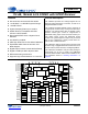
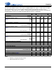
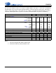
Table Of Contents
- 1. Characteristics and Specifications
- Specified Operating Conditions
- Absolute Maximum Ratings
- Analog Input Characteristics
- A/D Digital Filter Characteristics
- Analog Output Characteristics
- D/A Digital Filter Characteristics
- Switching Characteristics
- Switching Characteristics - Control Port - I²C™ Format
- Switching Characteristics - Control Port - SPI™ Format
- DC Electrical Characteristics
- Digital Interface Characteristics
- 2. Pin Descriptions
- 3. Typical Connection Diagram
- 4. Applications
- 4.1 Overview
- 4.2 Analog Inputs
- 4.3 Analog Outputs
- 4.4 S/PDIF Receiver
- 4.5 Clock Generation
- 4.6 Digital Interfaces
- 4.7 Control Port Description and Timing
- 4.8 Interrupts
- 4.9 Reset and Power-Up
- 4.10 Power Supply, Grounding, and PCB Layout
- 5. Register Quick Reference
- 6. Register Description
- Table 5. DAC De-Emphasis
- Table 6. Receiver De-Emphasis
- Table 7. Digital Interface Formats
- Table 8. ADC One-Line Mode
- Table 9. DAC One-Line Mode
- Table 10. RMCK Divider Settings
- Table 11. OMCK Frequency Settings
- Table 12. Master Clock Source Select
- Table 13. AES Format Detection
- Table 14. Receiver Clock Frequency Detection
- Table 15. Example Digital Volume Settings
- Table 16. ATAPI Decode
- Table 17. Example ADC Input Gain Settings
- Table 18. TXP Output Selection
- Table 19. Receiver Input Selection
- Table 20. Auxiliary Data Width Selection
- 7. Parameter Definitions
- 8. Appendix A: External Filters
- 9. Appendix B: S/PDIF Receiver
- 10. Appendix C: PLL Filter
- 11. Appendix D: External AES3-S/PDIF-IEC60958 Receiver Components
- 12. Appendix E: ADC Filter Plots
- Figure 34. Single-Speed Mode Stopband Rejection
- Figure 35. Single-Speed Mode Transition Band
- Figure 36. Single-Speed Mode Transition Band (Detail)
- Figure 37. Single-Speed Mode Passband Ripple
- Figure 38. Double-Speed Mode Stopband Rejection
- Figure 39. Double-Speed Mode Transition Band
- Figure 40. Double-Speed Mode Transition Band (Detail)
- Figure 41. Double-Speed Mode Passband Ripple
- Figure 42. Quad-Speed Mode Stopband Rejection
- Figure 43. Quad-Speed Mode Transition Band
- Figure 44. Quad-Speed Mode Transition Band (Detail)
- Figure 45. Quad-Speed Mode Passband Ripple
- 13. Appendix F: DAC Filter Plots
- Figure 46. Single-Speed (fast) Stopband Rejection
- Figure 47. Single-Speed (fast) Transition Band
- Figure 48. Single-Speed (fast) Transition Band (detail)
- Figure 49. Single-Speed (fast) Passband Ripple
- Figure 50. Single-Speed (slow) Stopband Rejection
- Figure 51. Single-Speed (slow) Transition Band
- Figure 52. Single-Speed (slow) Transition Band (detail)
- Figure 53. Single-Speed (slow) Passband Ripple
- Figure 54. Double-Speed (fast) Stopband Rejection
- Figure 55. Double-Speed (fast) Transition Band
- Figure 56. Double-Speed (fast) Transition Band (detail)
- Figure 57. Double-Speed (fast) Passband Ripple
- Figure 58. Double-Speed (slow) Stopband Rejection
- Figure 59. Double-Speed (slow) Transition Band
- Figure 60. Double-Speed (slow) Transition Band (detail)
- Figure 61. Double-Speed (slow) Passband Ripple
- Figure 62. Quad-Speed (fast) Stopband Rejection
- Figure 63. Quad-Speed (fast) Transition Band
- Figure 64. Quad-Speed (fast) Transition Band (detail)
- Figure 65. Quad-Speed (fast) Passband Ripple
- Figure 66. Quad-Speed (slow) Stopband Rejection
- Figure 67. Quad-Speed (slow) Transition Band
- Figure 68. Quad-Speed (slow) Transition Band (detail)
- Figure 69. Quad-Speed (slow) Passband Ripple
- 14. Package Dimensions
- 15. Ordering Information
- 16. References
- 17. Revision History
DS583F2 9
CS42516
ANALOG OUTPUT CHARACTERISTICS
(T
A
= 25° C; VA =VARX= 5 V, VD = 3.3 V, Logic “0” = DGND =AGND = 0 V; Logic “1” = VLS = VLC = 5V; Measure-
ment Bandwidth 10 Hz to 20 kHz unless otherwise specified.; Full-scale output 997 Hz sine wave, Test load R
L
=
3k, C
L
= 30 pF; PDN_RCVR = 1; SW_CTRL[1:0] = ‘01’; OMCK = 12.288 MHz; Single-Speed Mode, CX_SCLK =
3.072 MHz; Double-Speed Mode, CX_SCLK = 6.144 MHz; Quad-Speed Mode, CX_SCLK = 12.288 MHz.)
Notes:
7. One LSB of triangular PDF dither is added to data.
8. Performance limited by 16-bit quantization noise.
Parameter Symbol Min Typ Max Unit
Dynamic performance for all modes
Dynamic Range (Note 7)
24-bit A-Weighted
unweighted
16-bit A-Weighted
(Note 8) unweighted
104
101
-
-
110
107
97
94
-
-
-
-
dB
dB
dB
dB
Total Harmonic Distortion + Noise
24-bit 0 dB
-20 dB
-60 dB
16-bit 0 dB
(Note 8) -20 dB
-60 dB
THD+N
-
-
-
-
-
-
-100
-91
-51
-94
-74
-34
-94
-
-
-
-
dB
dB
dB
dB
dB
dB
Idle Channel Noise/Signal-to-Noise Ratio (A-Weighted)
-110 - dB
Interchannel Isolation (1 kHz)
-90 -dB
Analog Output Characteristics for all modes
Unloaded Full-Scale Differential Output Voltage
V
FS
.89 VA .94 VA .99 VA Vpp
Interchannel Gain Mismatch
-0.1 - dB
Gain Drift
- 300 - ppm/°C
Output Impedance
Z
OUT
- 150 -
AC-Load Resistance
R
L
3- -k
Load Capacitance
C
L
- - 30 pF