
User guide
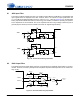
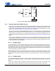
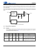
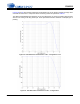

Table Of Contents
- 1. Characteristics and Specifications
- Specified Operating Conditions
- Absolute Maximum Ratings
- Analog Input Characteristics
- A/D Digital Filter Characteristics
- Analog Output Characteristics
- D/A Digital Filter Characteristics
- Switching Characteristics
- Switching Characteristics - Control Port - I²C™ Format
- Switching Characteristics - Control Port - SPI™ Format
- DC Electrical Characteristics
- Digital Interface Characteristics
- 2. Pin Descriptions
- 3. Typical Connection Diagram
- 4. Applications
- 4.1 Overview
- 4.2 Analog Inputs
- 4.3 Analog Outputs
- 4.4 S/PDIF Receiver
- 4.5 Clock Generation
- 4.6 Digital Interfaces
- 4.7 Control Port Description and Timing
- 4.8 Interrupts
- 4.9 Reset and Power-Up
- 4.10 Power Supply, Grounding, and PCB Layout
- 5. Register Quick Reference
- 6. Register Description
- Table 5. DAC De-Emphasis
- Table 6. Receiver De-Emphasis
- Table 7. Digital Interface Formats
- Table 8. ADC One-Line Mode
- Table 9. DAC One-Line Mode
- Table 10. RMCK Divider Settings
- Table 11. OMCK Frequency Settings
- Table 12. Master Clock Source Select
- Table 13. AES Format Detection
- Table 14. Receiver Clock Frequency Detection
- Table 15. Example Digital Volume Settings
- Table 16. ATAPI Decode
- Table 17. Example ADC Input Gain Settings
- Table 18. TXP Output Selection
- Table 19. Receiver Input Selection
- Table 20. Auxiliary Data Width Selection
- 7. Parameter Definitions
- 8. Appendix A: External Filters
- 9. Appendix B: S/PDIF Receiver
- 10. Appendix C: PLL Filter
- 11. Appendix D: External AES3-S/PDIF-IEC60958 Receiver Components
- 12. Appendix E: ADC Filter Plots
- Figure 34. Single-Speed Mode Stopband Rejection
- Figure 35. Single-Speed Mode Transition Band
- Figure 36. Single-Speed Mode Transition Band (Detail)
- Figure 37. Single-Speed Mode Passband Ripple
- Figure 38. Double-Speed Mode Stopband Rejection
- Figure 39. Double-Speed Mode Transition Band
- Figure 40. Double-Speed Mode Transition Band (Detail)
- Figure 41. Double-Speed Mode Passband Ripple
- Figure 42. Quad-Speed Mode Stopband Rejection
- Figure 43. Quad-Speed Mode Transition Band
- Figure 44. Quad-Speed Mode Transition Band (Detail)
- Figure 45. Quad-Speed Mode Passband Ripple
- 13. Appendix F: DAC Filter Plots
- Figure 46. Single-Speed (fast) Stopband Rejection
- Figure 47. Single-Speed (fast) Transition Band
- Figure 48. Single-Speed (fast) Transition Band (detail)
- Figure 49. Single-Speed (fast) Passband Ripple
- Figure 50. Single-Speed (slow) Stopband Rejection
- Figure 51. Single-Speed (slow) Transition Band
- Figure 52. Single-Speed (slow) Transition Band (detail)
- Figure 53. Single-Speed (slow) Passband Ripple
- Figure 54. Double-Speed (fast) Stopband Rejection
- Figure 55. Double-Speed (fast) Transition Band
- Figure 56. Double-Speed (fast) Transition Band (detail)
- Figure 57. Double-Speed (fast) Passband Ripple
- Figure 58. Double-Speed (slow) Stopband Rejection
- Figure 59. Double-Speed (slow) Transition Band
- Figure 60. Double-Speed (slow) Transition Band (detail)
- Figure 61. Double-Speed (slow) Passband Ripple
- Figure 62. Quad-Speed (fast) Stopband Rejection
- Figure 63. Quad-Speed (fast) Transition Band
- Figure 64. Quad-Speed (fast) Transition Band (detail)
- Figure 65. Quad-Speed (fast) Passband Ripple
- Figure 66. Quad-Speed (slow) Stopband Rejection
- Figure 67. Quad-Speed (slow) Transition Band
- Figure 68. Quad-Speed (slow) Transition Band (detail)
- Figure 69. Quad-Speed (slow) Passband Ripple
- 14. Package Dimensions
- 15. Ordering Information
- 16. References
- 17. Revision History
DS583F2 75
CS42516
9.2.1 Channel Status Data E Buffer Access
The user can monitor the incoming Channel Status data by reading the E buffer, which is mapped into the
register space of the CS42516 through the control port Data Buffer. The Data Buffer must first be config-
ured to point to the address space of the C data. This is accomplished by setting the BSEL bit to ‘0’ in the
register “Channel Status Data Buffer Control (address 24h)” on page 65.
The user can configure the Interrupt Mask Register to cause an interrupt whenever any data-bit changes
are detected when D to E Channel Status buffer transfers occur. If no data bits have changed within the
current transfer of data from D to E, no interrupt will be generated. This allows determination of the ac-
ceptable time periods to interact with the E buffer. See “Interrupt Mask (address 21h)” on page 64 for more
details.
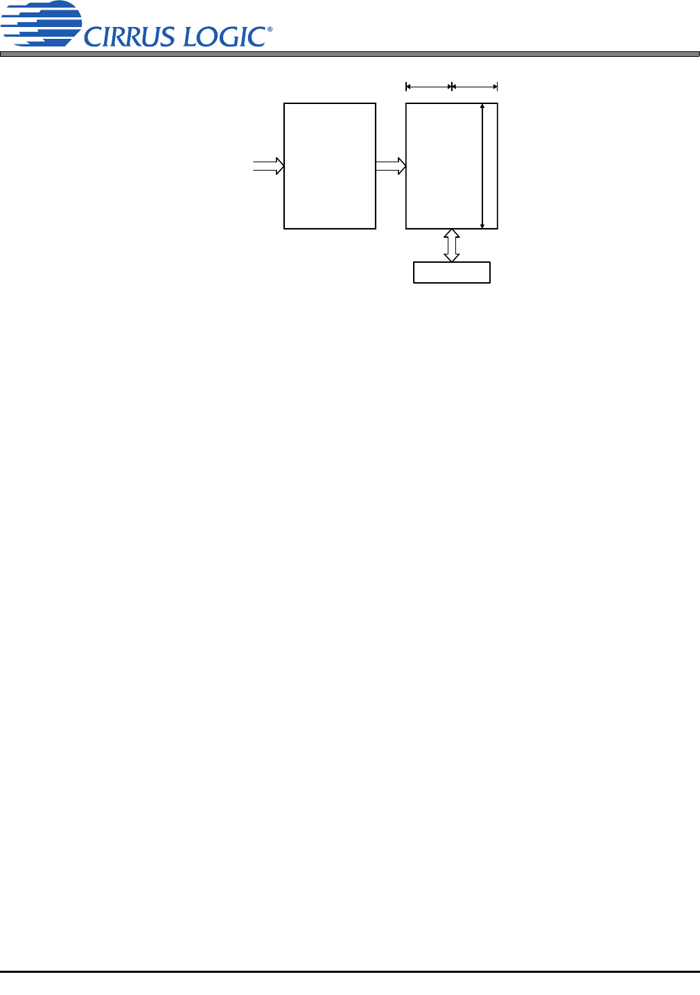
The E buffer is organized as 24 x 16-bit words. For each word the MS Byte is the A channel data, and the
LS Byte is the B channel data (see Figure 26). There are two methods of accessing this memory, known
as One-Byte Mode and Two-Byte Mode. The desired mode is selected by setting the CAM bit in the Chan-
nel Status Data Buffer Control Register.
9.2.1.1 One-Byte Mode
In many applications, the channel status blocks for the A and B channels will be identical. In this situation,
the user may read a byte from one of the channel's blocks since the corresponding byte for the other chan-
nel will likely be the same. One-Byte Mode takes advantage of the often identical nature of A and B channel
status data. When reading data in One-Byte Mode, a single byte is returned, which can be from channel A
or B data, depending on a register control bit.
One-Byte Mode saves the user substantial control port access time, as it effectively accesses two bytes
worth of information in 1 byte's worth of access time. If the control port's auto-increment addressing is used
in combination with this mode, multi-byte accesses, such as full-block reads, can be done especially effi-
ciently.
9.2.1.2 Two-Byte Mode
There are those applications in which the A and B channel status blocks will not be the same, and the user
is interested in accessing both blocks. In these situations, Two-Byte Mode should be used to access the
E buffer.
In this mode, a read will cause the CS42516 to output two bytes from its control port. The first byte out will
represent the A channel status data, and the second byte will represent the B channel status data.
Control Port
From
S/PDIF
Receiver
E
24
words
8-bits 8-bits
AB
D
Received
Data
Buffer
Figure 26. Channel Status Data Buffer Structure