
User guide
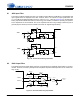
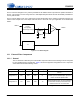

Table Of Contents
- 1. Characteristics and Specifications
- Specified Operating Conditions
- Absolute Maximum Ratings
- Analog Input Characteristics
- A/D Digital Filter Characteristics
- Analog Output Characteristics
- D/A Digital Filter Characteristics
- Switching Characteristics
- Switching Characteristics - Control Port - I²C™ Format
- Switching Characteristics - Control Port - SPI™ Format
- DC Electrical Characteristics
- Digital Interface Characteristics
- 2. Pin Descriptions
- 3. Typical Connection Diagram
- 4. Applications
- 4.1 Overview
- 4.2 Analog Inputs
- 4.3 Analog Outputs
- 4.4 S/PDIF Receiver
- 4.5 Clock Generation
- 4.6 Digital Interfaces
- 4.7 Control Port Description and Timing
- 4.8 Interrupts
- 4.9 Reset and Power-Up
- 4.10 Power Supply, Grounding, and PCB Layout
- 5. Register Quick Reference
- 6. Register Description
- Table 5. DAC De-Emphasis
- Table 6. Receiver De-Emphasis
- Table 7. Digital Interface Formats
- Table 8. ADC One-Line Mode
- Table 9. DAC One-Line Mode
- Table 10. RMCK Divider Settings
- Table 11. OMCK Frequency Settings
- Table 12. Master Clock Source Select
- Table 13. AES Format Detection
- Table 14. Receiver Clock Frequency Detection
- Table 15. Example Digital Volume Settings
- Table 16. ATAPI Decode
- Table 17. Example ADC Input Gain Settings
- Table 18. TXP Output Selection
- Table 19. Receiver Input Selection
- Table 20. Auxiliary Data Width Selection
- 7. Parameter Definitions
- 8. Appendix A: External Filters
- 9. Appendix B: S/PDIF Receiver
- 10. Appendix C: PLL Filter
- 11. Appendix D: External AES3-S/PDIF-IEC60958 Receiver Components
- 12. Appendix E: ADC Filter Plots
- Figure 34. Single-Speed Mode Stopband Rejection
- Figure 35. Single-Speed Mode Transition Band
- Figure 36. Single-Speed Mode Transition Band (Detail)
- Figure 37. Single-Speed Mode Passband Ripple
- Figure 38. Double-Speed Mode Stopband Rejection
- Figure 39. Double-Speed Mode Transition Band
- Figure 40. Double-Speed Mode Transition Band (Detail)
- Figure 41. Double-Speed Mode Passband Ripple
- Figure 42. Quad-Speed Mode Stopband Rejection
- Figure 43. Quad-Speed Mode Transition Band
- Figure 44. Quad-Speed Mode Transition Band (Detail)
- Figure 45. Quad-Speed Mode Passband Ripple
- 13. Appendix F: DAC Filter Plots
- Figure 46. Single-Speed (fast) Stopband Rejection
- Figure 47. Single-Speed (fast) Transition Band
- Figure 48. Single-Speed (fast) Transition Band (detail)
- Figure 49. Single-Speed (fast) Passband Ripple
- Figure 50. Single-Speed (slow) Stopband Rejection
- Figure 51. Single-Speed (slow) Transition Band
- Figure 52. Single-Speed (slow) Transition Band (detail)
- Figure 53. Single-Speed (slow) Passband Ripple
- Figure 54. Double-Speed (fast) Stopband Rejection
- Figure 55. Double-Speed (fast) Transition Band
- Figure 56. Double-Speed (fast) Transition Band (detail)
- Figure 57. Double-Speed (fast) Passband Ripple
- Figure 58. Double-Speed (slow) Stopband Rejection
- Figure 59. Double-Speed (slow) Transition Band
- Figure 60. Double-Speed (slow) Transition Band (detail)
- Figure 61. Double-Speed (slow) Passband Ripple
- Figure 62. Quad-Speed (fast) Stopband Rejection
- Figure 63. Quad-Speed (fast) Transition Band
- Figure 64. Quad-Speed (fast) Transition Band (detail)
- Figure 65. Quad-Speed (fast) Passband Ripple
- Figure 66. Quad-Speed (slow) Stopband Rejection
- Figure 67. Quad-Speed (slow) Transition Band
- Figure 68. Quad-Speed (slow) Transition Band (detail)
- Figure 69. Quad-Speed (slow) Passband Ripple
- 14. Package Dimensions
- 15. Ordering Information
- 16. References
- 17. Revision History
74 DS583F2
CS42516
9. APPENDIX B: S/PDIF RECEIVER
9.1 Error Reporting and Hold Function
The UNLOCK bit indicates whether the PLL is locked to the incoming S/PDIF data. The V bit reflects the
current validity bit status. The CONF (Confidence) bit indicates the amplitude of the eye pattern opening,
indicating a link that is close to generating errors. The BIP (Bi-Phase) error bit indicates an error in incoming
bi-phase coding. The PAR (Parity) bit indicates a received parity error.
The error bits are “sticky”, meaning they are set on the first occurrence of the associated error and will re-
main set until the user reads the register through the control port. This enables the register to log all un-
masked errors that occurred since the last time the register was read.
The Receiver Errors Mask register (See “Receiver Errors Mask (address 27h)” on page 68) allows masking
of individual errors. The bits in this register serve as masks for the corresponding bits of the Receiver Error
Register. If a mask bit is set to 1, the error is unmasked, which implies the following: its occurrence will be
reported in the receiver error register, invoke the occurrence of a RERR interrupt, and affect the current au-
dio sample according to the status of the HOLD bits. The HOLD bits allow a choice of holding the previous
sample, replacing the current sample with zero (mute), or not changing the current audio sample. If a mask
bit is set to 0, the error is masked, which implies the following: its occurrence will not be reported in the re-
ceiver error register, the RERR interrupt will not be generated, and the current audio sample will not be af-
fected. The QCRC and CCRC errors do not affect the current audio sample, even if unmasked.
9.2 Channel Status Data Handling
The setting of the CHS bit in the register “Channel Status Data Buffer Control (address 24h)” on page 65
determines whether the channel status decodes are from the A channel (CHS = 0) or B channel (CHS = 1).
The PRO (professional) bit is extracted directly. For consumer data, the COPY (copyright) bit is extracted,
and the category code and L bits are decoded to determine SCMS status, indicated by the ORIG (original)
bit. If the category code is set to General on the incoming S/PDIF stream, copyright will always be indicated
even when the stream indicates no copyright. Finally, the AUDIO
bit is extracted and used to set an AUDIO
indicator, as described in section 4.4.5, Non-Audio Auto-Detection.
If 50/15 µs pre-emphasis is detected, and the Receiver Auto De-emphasis control is enabled, then de-em-
phasis will automatically be applied to the incoming digital PCM data. See “Functional Mode (address 03h)”
on page 47 for more details.
The encoded channel status bits which indicate sample word length are decoded according to IEC 60958.
Audio data routed to the Serial Audio Interface port is unaffected by the word length settings; all 24 bits are
passed on as received.
The CS42516 also contains sufficient RAM to store a full block of C data for both A and B channels
(192 x 2 = 384 bits), and also 384 bits of User (U data) information. The user may read from these buffer
RAMs through the control port.
The buffering scheme involves two block-sized buffers, named D and E, as shown in Figure 26. The MSB
of each byte represents the first bit in the serial C data stream. For example, the MSB of byte 0 (which is at
control port address 4Ah) is the consumer/professional bit for channel status block A.
The first buffer (D) accepts incoming C data from the S/PDIF receiver. The 2nd buffer (E) accepts entire
blocks of data from the D buffer. The E buffer is also accessible from the control port, allowing reading of
the C data.