
User guide
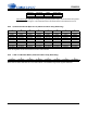
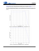

Table Of Contents
- 1. Characteristics and Specifications
- Specified Operating Conditions
- Absolute Maximum Ratings
- Analog Input Characteristics
- A/D Digital Filter Characteristics
- Analog Output Characteristics
- D/A Digital Filter Characteristics
- Switching Characteristics
- Switching Characteristics - Control Port - I²C™ Format
- Switching Characteristics - Control Port - SPI™ Format
- DC Electrical Characteristics
- Digital Interface Characteristics
- 2. Pin Descriptions
- 3. Typical Connection Diagram
- 4. Applications
- 4.1 Overview
- 4.2 Analog Inputs
- 4.3 Analog Outputs
- 4.4 S/PDIF Receiver
- 4.5 Clock Generation
- 4.6 Digital Interfaces
- 4.7 Control Port Description and Timing
- 4.8 Interrupts
- 4.9 Reset and Power-Up
- 4.10 Power Supply, Grounding, and PCB Layout
- 5. Register Quick Reference
- 6. Register Description
- Table 5. DAC De-Emphasis
- Table 6. Receiver De-Emphasis
- Table 7. Digital Interface Formats
- Table 8. ADC One-Line Mode
- Table 9. DAC One-Line Mode
- Table 10. RMCK Divider Settings
- Table 11. OMCK Frequency Settings
- Table 12. Master Clock Source Select
- Table 13. AES Format Detection
- Table 14. Receiver Clock Frequency Detection
- Table 15. Example Digital Volume Settings
- Table 16. ATAPI Decode
- Table 17. Example ADC Input Gain Settings
- Table 18. TXP Output Selection
- Table 19. Receiver Input Selection
- Table 20. Auxiliary Data Width Selection
- 7. Parameter Definitions
- 8. Appendix A: External Filters
- 9. Appendix B: S/PDIF Receiver
- 10. Appendix C: PLL Filter
- 11. Appendix D: External AES3-S/PDIF-IEC60958 Receiver Components
- 12. Appendix E: ADC Filter Plots
- Figure 34. Single-Speed Mode Stopband Rejection
- Figure 35. Single-Speed Mode Transition Band
- Figure 36. Single-Speed Mode Transition Band (Detail)
- Figure 37. Single-Speed Mode Passband Ripple
- Figure 38. Double-Speed Mode Stopband Rejection
- Figure 39. Double-Speed Mode Transition Band
- Figure 40. Double-Speed Mode Transition Band (Detail)
- Figure 41. Double-Speed Mode Passband Ripple
- Figure 42. Quad-Speed Mode Stopband Rejection
- Figure 43. Quad-Speed Mode Transition Band
- Figure 44. Quad-Speed Mode Transition Band (Detail)
- Figure 45. Quad-Speed Mode Passband Ripple
- 13. Appendix F: DAC Filter Plots
- Figure 46. Single-Speed (fast) Stopband Rejection
- Figure 47. Single-Speed (fast) Transition Band
- Figure 48. Single-Speed (fast) Transition Band (detail)
- Figure 49. Single-Speed (fast) Passband Ripple
- Figure 50. Single-Speed (slow) Stopband Rejection
- Figure 51. Single-Speed (slow) Transition Band
- Figure 52. Single-Speed (slow) Transition Band (detail)
- Figure 53. Single-Speed (slow) Passband Ripple
- Figure 54. Double-Speed (fast) Stopband Rejection
- Figure 55. Double-Speed (fast) Transition Band
- Figure 56. Double-Speed (fast) Transition Band (detail)
- Figure 57. Double-Speed (fast) Passband Ripple
- Figure 58. Double-Speed (slow) Stopband Rejection
- Figure 59. Double-Speed (slow) Transition Band
- Figure 60. Double-Speed (slow) Transition Band (detail)
- Figure 61. Double-Speed (slow) Passband Ripple
- Figure 62. Quad-Speed (fast) Stopband Rejection
- Figure 63. Quad-Speed (fast) Transition Band
- Figure 64. Quad-Speed (fast) Transition Band (detail)
- Figure 65. Quad-Speed (fast) Passband Ripple
- Figure 66. Quad-Speed (slow) Stopband Rejection
- Figure 67. Quad-Speed (slow) Transition Band
- Figure 68. Quad-Speed (slow) Transition Band (detail)
- Figure 69. Quad-Speed (slow) Passband Ripple
- 14. Package Dimensions
- 15. Ordering Information
- 16. References
- 17. Revision History
DS583F2 71
CS42516
following table. It is recommended that in this mode the remaining functional bits be set to 0.
GPO, Drive High - If the pin is configured as a general-purpose output, the functional bits are ignored
and the pin is driven high. It is recommended that in this mode all the functional bits be set to 0.
6.29 Q-Channel Subcode Bytes 0 to 9 (addresses 30h to 39h) (Read Only)
These ten registers contain the decoded Q-channel subcode data.
6.30 C-Bit or U-Bit Data Buffer (addresses 3Ah to 51h) (Read Only)
Either channel status data buffer E or user data buffer E is accessible through these register addresses.
Function1 Function0 GPOx Driver Type
0 0 Drive Low CMOS
1 1 OVFL R or L Open Drain
76543210
Address3 Address2 Address1 Address0 Control3 Control2 Control1 Control0
Track7 Track6 Track5 Track4 Track3 Track2 Track1 Track0
Index7 Index6 Index5 Index4 Index3 Index2 Index1 Index0
Minute7 Minute6 Minute5 Minute4 Minute3 Minute2 Minute1 Minute0
Second7 Second6 Second5 Second4 Second3 Second2 Second1 Second0
Frame7 Frame6 Frame5 Frame4 Frame3 Frame2 Frame1 Frame0
Zero7 Zero6 Zero5 Zero4 Zero3 Zero2 Zero1 Zero0
A.Minute7 A.Minute6 A.Minute5 A.Minute4 A.Minute3 A.Minute2 A.Minute1 A.Minute0
A.Second7 A.Second6 A.Second5 A.Second4 A.Second3 A.Second2 A.Second1 A.Second0
A.Frame7 A.Frame6 A.Frame5 A.Frame4 A.Frame3 A.Frame2 A.Frame1 A.Frame0
76543210
CU Buffer7 CU Buffer6 CU Buffer5 CU Buffer4 CU Buffer3 CU Buffer2 CU Buffer1 CU Buffer0