
User guide
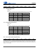
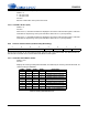
Table Of Contents
- 1. Characteristics and Specifications
- Specified Operating Conditions
- Absolute Maximum Ratings
- Analog Input Characteristics
- A/D Digital Filter Characteristics
- Analog Output Characteristics
- D/A Digital Filter Characteristics
- Switching Characteristics
- Switching Characteristics - Control Port - I²C™ Format
- Switching Characteristics - Control Port - SPI™ Format
- DC Electrical Characteristics
- Digital Interface Characteristics
- 2. Pin Descriptions
- 3. Typical Connection Diagram
- 4. Applications
- 4.1 Overview
- 4.2 Analog Inputs
- 4.3 Analog Outputs
- 4.4 S/PDIF Receiver
- 4.5 Clock Generation
- 4.6 Digital Interfaces
- 4.7 Control Port Description and Timing
- 4.8 Interrupts
- 4.9 Reset and Power-Up
- 4.10 Power Supply, Grounding, and PCB Layout
- 5. Register Quick Reference
- 6. Register Description
- Table 5. DAC De-Emphasis
- Table 6. Receiver De-Emphasis
- Table 7. Digital Interface Formats
- Table 8. ADC One-Line Mode
- Table 9. DAC One-Line Mode
- Table 10. RMCK Divider Settings
- Table 11. OMCK Frequency Settings
- Table 12. Master Clock Source Select
- Table 13. AES Format Detection
- Table 14. Receiver Clock Frequency Detection
- Table 15. Example Digital Volume Settings
- Table 16. ATAPI Decode
- Table 17. Example ADC Input Gain Settings
- Table 18. TXP Output Selection
- Table 19. Receiver Input Selection
- Table 20. Auxiliary Data Width Selection
- 7. Parameter Definitions
- 8. Appendix A: External Filters
- 9. Appendix B: S/PDIF Receiver
- 10. Appendix C: PLL Filter
- 11. Appendix D: External AES3-S/PDIF-IEC60958 Receiver Components
- 12. Appendix E: ADC Filter Plots
- Figure 34. Single-Speed Mode Stopband Rejection
- Figure 35. Single-Speed Mode Transition Band
- Figure 36. Single-Speed Mode Transition Band (Detail)
- Figure 37. Single-Speed Mode Passband Ripple
- Figure 38. Double-Speed Mode Stopband Rejection
- Figure 39. Double-Speed Mode Transition Band
- Figure 40. Double-Speed Mode Transition Band (Detail)
- Figure 41. Double-Speed Mode Passband Ripple
- Figure 42. Quad-Speed Mode Stopband Rejection
- Figure 43. Quad-Speed Mode Transition Band
- Figure 44. Quad-Speed Mode Transition Band (Detail)
- Figure 45. Quad-Speed Mode Passband Ripple
- 13. Appendix F: DAC Filter Plots
- Figure 46. Single-Speed (fast) Stopband Rejection
- Figure 47. Single-Speed (fast) Transition Band
- Figure 48. Single-Speed (fast) Transition Band (detail)
- Figure 49. Single-Speed (fast) Passband Ripple
- Figure 50. Single-Speed (slow) Stopband Rejection
- Figure 51. Single-Speed (slow) Transition Band
- Figure 52. Single-Speed (slow) Transition Band (detail)
- Figure 53. Single-Speed (slow) Passband Ripple
- Figure 54. Double-Speed (fast) Stopband Rejection
- Figure 55. Double-Speed (fast) Transition Band
- Figure 56. Double-Speed (fast) Transition Band (detail)
- Figure 57. Double-Speed (fast) Passband Ripple
- Figure 58. Double-Speed (slow) Stopband Rejection
- Figure 59. Double-Speed (slow) Transition Band
- Figure 60. Double-Speed (slow) Transition Band (detail)
- Figure 61. Double-Speed (slow) Passband Ripple
- Figure 62. Quad-Speed (fast) Stopband Rejection
- Figure 63. Quad-Speed (fast) Transition Band
- Figure 64. Quad-Speed (fast) Transition Band (detail)
- Figure 65. Quad-Speed (fast) Passband Ripple
- Figure 66. Quad-Speed (slow) Stopband Rejection
- Figure 67. Quad-Speed (slow) Transition Band
- Figure 68. Quad-Speed (slow) Transition Band (detail)
- Figure 69. Quad-Speed (slow) Passband Ripple
- 14. Package Dimensions
- 15. Ordering Information
- 16. References
- 17. Revision History
70 DS583F2
CS42516
or as a dedicated ADC overflow pin indicating an over-range condition anywhere in the ADC signal
path for either the left or right channel. The Functionx bits determine the operation of the pin. When
configured as a GPO with the output driven low, the driver is a CMOS driver. When configured to iden-
tify an ADC Overflow condition, the driver is an open drain driver requiring a pull-up resistor.
GPO, Drive High Mode
- The pin is configured as a general purpose output driven high.
6.28.2 POLARITY SELECT (POLARITY)
Default = 0
Function:
RXP Input
- If the pin is configured for an RXP input, the polarity bit is ignored. It is recommended that
in this mode this bit be set to 0.
Mute Mode
- If the pin is configured as a dedicated mute output pin, the polarity bit determines the
polarity of the mapped pin according to the following
0 - Active low
1 - Active high
GPO, Drive Low / ADC Overflow Mode
- If the pin is configured as a GPO, Drive Low / ADC Overflow
Mode pin, the polarity bit is ignored. It is recommended that in this mode this bit be set to 0.
GPO, Drive High
- If the pin is configured as a general-purpose output driven high, the polarity bit is
ignored. It is recommended that in this mode this bit be set to 0.
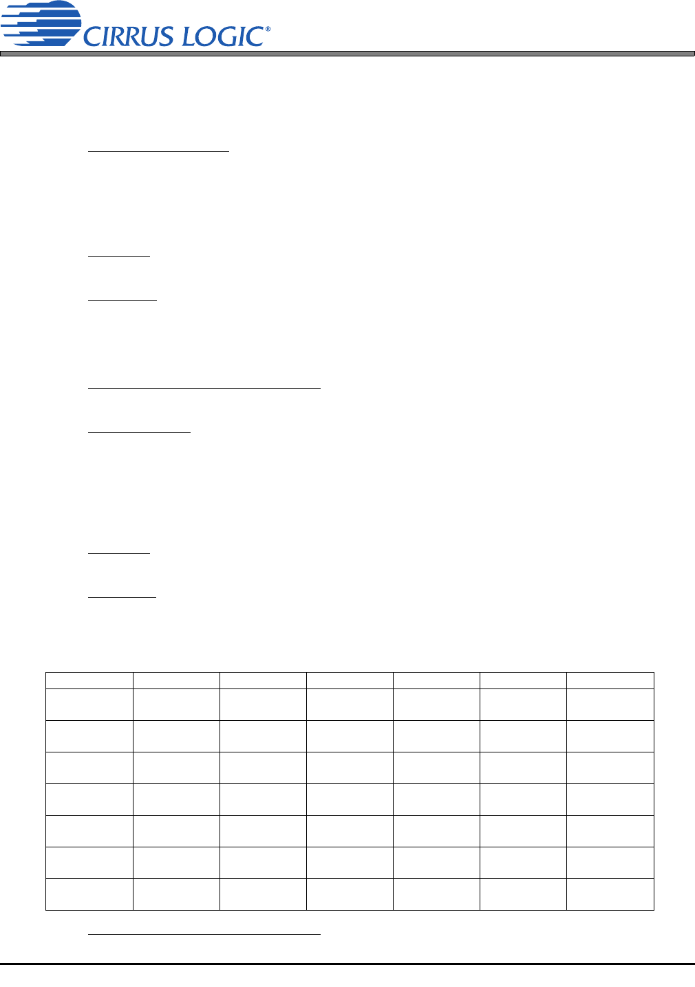
6.28.3 FUNCTIONAL CONTROL (FUNCTIONX)
Default = 00000
Function:
RXP Input
- If the pin is configured for an RXP input, the functional bits are ignored. It is recommended
that in this mode all the functional bits be set to 0.
Mute Mode
- If the pin is configured as a dedicated mute pin, the functional bits determine which chan-
nel mutes will be mapped to this pin according to the following table.
0 - Channel mute is not mapped to the RXPx/GPOx pin
1 - Channel mute is mapped to the RXPx/GPOx pin:
GPO, Drive Low / ADC Overflow Mode
- If the pin is configured as a GPO, Drive Low / ADC Overflow
Mode pin, the Function1 and Function0 bits determine how the output will behave according to the
RXPx/GPOx Reg Address Function4 Function3 Function2 Function1 Function0
RXP7/GPO7
pin 42
29h M_AOUTA1 M_AOUTB1
M_AOUTA2
M_AOUTB2
M_AOUTA3
M_AOUTB3
Reserved
RXP6/GPO6
pin 43
2Ah
M_AOUTA1
M_AOUTB1
M_AOUTA2 M_AOUTB2
M_AOUTA3
M_AOUTB3
Reserved
RXP5/GPO5
pin 44
2Bh
M_AOUTA1
M_AOUTB1
M_AOUTA2 M_AOUTB2
M_AOUTA3
M_AOUTB3
Reserved
RXP4/GPO4
pin 45
2Ch
M_AOUTA1
M_AOUTB1
M_AOUTA2
M_AOUTB2
M_AOUTA3 M_AOUTB3 Reserved
RXP3/GPO3
pin 46
2Dh
M_AOUTA1
M_AOUTB1
M_AOUTA2
M_AOUTB2
M_AOUTA3 M_AOUTB3 Reserved
RXP2/GPO2
pin 47
2Eh
M_AOUTA1
M_AOUTB1
M_AOUTA2
M_AOUTB2
M_AOUTA3
M_AOUTB3
Reserved Reserved
RXP1/GPO1
pin 48
2Fh
M_AOUTA1
M_AOUTB1
M_AOUTA2
M_AOUTB2
M_AOUTA3
M_AOUTB3
Reserved Reserved