
User guide
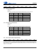
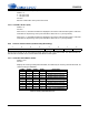
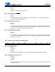
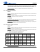
Table Of Contents
- 1. Characteristics and Specifications
- Specified Operating Conditions
- Absolute Maximum Ratings
- Analog Input Characteristics
- A/D Digital Filter Characteristics
- Analog Output Characteristics
- D/A Digital Filter Characteristics
- Switching Characteristics
- Switching Characteristics - Control Port - I²C™ Format
- Switching Characteristics - Control Port - SPI™ Format
- DC Electrical Characteristics
- Digital Interface Characteristics
- 2. Pin Descriptions
- 3. Typical Connection Diagram
- 4. Applications
- 4.1 Overview
- 4.2 Analog Inputs
- 4.3 Analog Outputs
- 4.4 S/PDIF Receiver
- 4.5 Clock Generation
- 4.6 Digital Interfaces
- 4.7 Control Port Description and Timing
- 4.8 Interrupts
- 4.9 Reset and Power-Up
- 4.10 Power Supply, Grounding, and PCB Layout
- 5. Register Quick Reference
- 6. Register Description
- Table 5. DAC De-Emphasis
- Table 6. Receiver De-Emphasis
- Table 7. Digital Interface Formats
- Table 8. ADC One-Line Mode
- Table 9. DAC One-Line Mode
- Table 10. RMCK Divider Settings
- Table 11. OMCK Frequency Settings
- Table 12. Master Clock Source Select
- Table 13. AES Format Detection
- Table 14. Receiver Clock Frequency Detection
- Table 15. Example Digital Volume Settings
- Table 16. ATAPI Decode
- Table 17. Example ADC Input Gain Settings
- Table 18. TXP Output Selection
- Table 19. Receiver Input Selection
- Table 20. Auxiliary Data Width Selection
- 7. Parameter Definitions
- 8. Appendix A: External Filters
- 9. Appendix B: S/PDIF Receiver
- 10. Appendix C: PLL Filter
- 11. Appendix D: External AES3-S/PDIF-IEC60958 Receiver Components
- 12. Appendix E: ADC Filter Plots
- Figure 34. Single-Speed Mode Stopband Rejection
- Figure 35. Single-Speed Mode Transition Band
- Figure 36. Single-Speed Mode Transition Band (Detail)
- Figure 37. Single-Speed Mode Passband Ripple
- Figure 38. Double-Speed Mode Stopband Rejection
- Figure 39. Double-Speed Mode Transition Band
- Figure 40. Double-Speed Mode Transition Band (Detail)
- Figure 41. Double-Speed Mode Passband Ripple
- Figure 42. Quad-Speed Mode Stopband Rejection
- Figure 43. Quad-Speed Mode Transition Band
- Figure 44. Quad-Speed Mode Transition Band (Detail)
- Figure 45. Quad-Speed Mode Passband Ripple
- 13. Appendix F: DAC Filter Plots
- Figure 46. Single-Speed (fast) Stopband Rejection
- Figure 47. Single-Speed (fast) Transition Band
- Figure 48. Single-Speed (fast) Transition Band (detail)
- Figure 49. Single-Speed (fast) Passband Ripple
- Figure 50. Single-Speed (slow) Stopband Rejection
- Figure 51. Single-Speed (slow) Transition Band
- Figure 52. Single-Speed (slow) Transition Band (detail)
- Figure 53. Single-Speed (slow) Passband Ripple
- Figure 54. Double-Speed (fast) Stopband Rejection
- Figure 55. Double-Speed (fast) Transition Band
- Figure 56. Double-Speed (fast) Transition Band (detail)
- Figure 57. Double-Speed (fast) Passband Ripple
- Figure 58. Double-Speed (slow) Stopband Rejection
- Figure 59. Double-Speed (slow) Transition Band
- Figure 60. Double-Speed (slow) Transition Band (detail)
- Figure 61. Double-Speed (slow) Passband Ripple
- Figure 62. Quad-Speed (fast) Stopband Rejection
- Figure 63. Quad-Speed (fast) Transition Band
- Figure 64. Quad-Speed (fast) Transition Band (detail)
- Figure 65. Quad-Speed (fast) Passband Ripple
- Figure 66. Quad-Speed (slow) Stopband Rejection
- Figure 67. Quad-Speed (slow) Transition Band
- Figure 68. Quad-Speed (slow) Transition Band (detail)
- Figure 69. Quad-Speed (slow) Passband Ripple
- 14. Package Dimensions
- 15. Ordering Information
- 16. References
- 17. Revision History
DS583F2 69
CS42516
the status of the HOLD bit. If a mask bit is set to 0, the error is masked, meaning that its occurrence
will not appear in the receiver error register, will not affect the RERR interrupt, and will not affect the
current audio sample. The CCRC and QCRC bits behave differently from the other bits: they do not
affect the current audio sample even when unmasked.
6.27 Mutec Pin Control (address 28h)
6.27.1 MUTEC POLARITY SELECT (MCPOLARITY)
Default = 0
0 - Active low
1 - Active high
Function:
Determines the polarity of the MUTEC pin.
6.27.2 CHANNEL MUTES SELECT (M_AOUTXX)
Default = 1111
0 - Channel mute is not mapped to the MUTEC pin
1 - Channel mute is mapped to the MUTEC pin
Function:
Determines which channel mutes will be mapped to the MUTEC pin. If no channel mute bits are
mapped, then the MUTEC pin is driven to the “active” state as defined by the POLARITY bit. These
Channel Mute Select bits are “ANDed” together in order for the MUTEC pin to go active. This means
that if multiple Channel Mutes are selected to be mapped to the MUTEC pin, all corresponding chan-
nels must be muted before the MUTEC will go active.
6.28 RXP/General-Purpose Pin Control (addresses 29h to 2Fh)
6.28.1 MODE CONTROL (MODEX)
Default = 00
00 - RXP Input
01 - Mute Mode
10 - GPO/Overflow Mode
11 - GPO, Drive High Mode
Function:
RXP Input
- The pin is configured as a receiver input which can then be muxed to either the TXP pin
or to the internal receiver.
Mute Mode
- The pin is configured as a dedicated mute pin. The muting function is controlled by the
Function bits.
GPO, Drive Low / ADC Overflow Mode
- The pin is configured as a general-purpose output driven low
76543210
Reserved Reserved MCPolarity M_AOUTA1 M_AOUTB1 M_AOUTA2
M_AOUTB2
M_AOUTA3
M_AOUTB3
Reserved
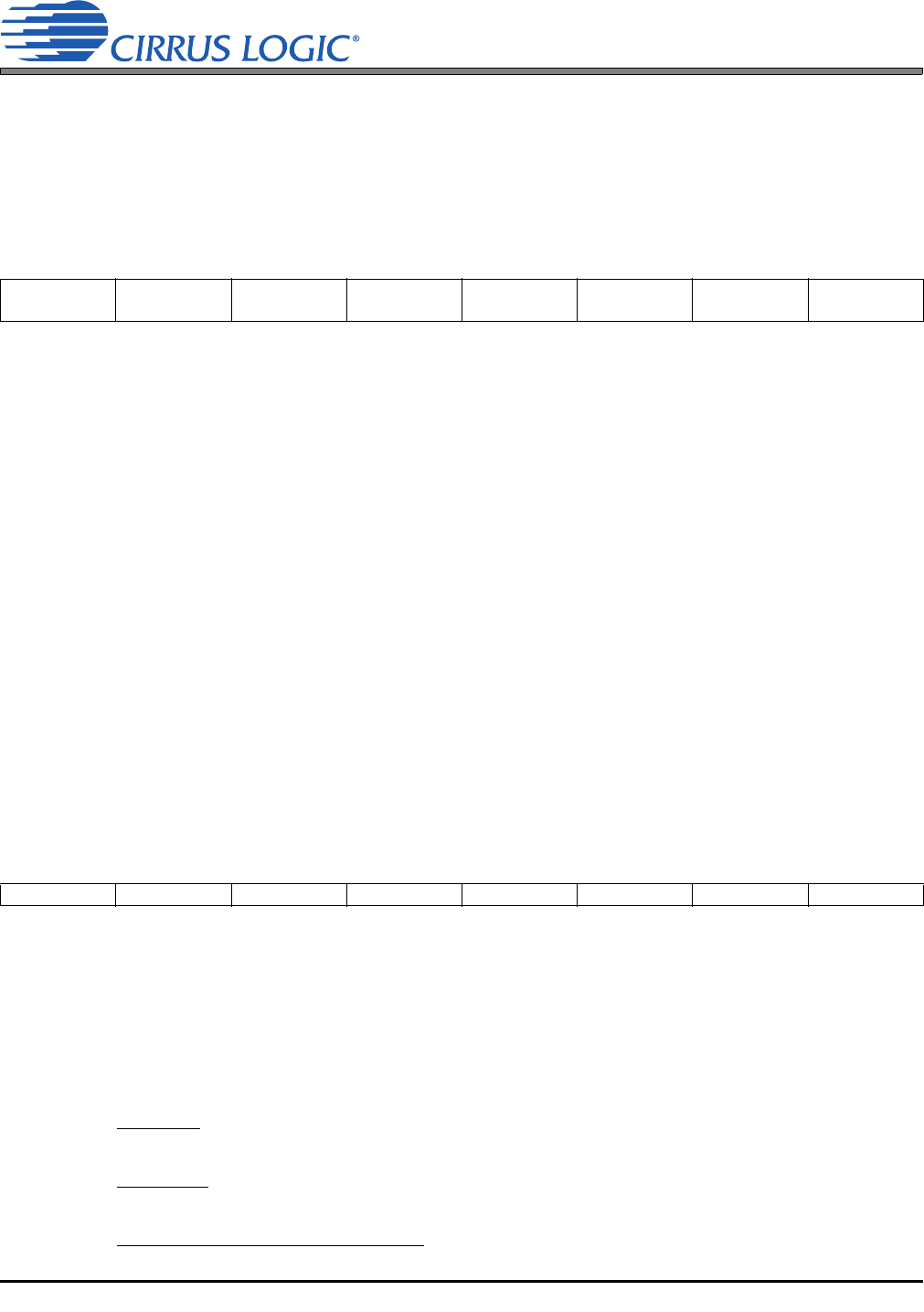
76543210
Mode1 Mode0 Polarity Function4 Function3 Function2 Function1 Function0