
User guide
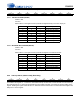
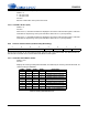
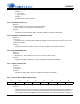
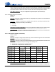
Table Of Contents
- 1. Characteristics and Specifications
- Specified Operating Conditions
- Absolute Maximum Ratings
- Analog Input Characteristics
- A/D Digital Filter Characteristics
- Analog Output Characteristics
- D/A Digital Filter Characteristics
- Switching Characteristics
- Switching Characteristics - Control Port - I²C™ Format
- Switching Characteristics - Control Port - SPI™ Format
- DC Electrical Characteristics
- Digital Interface Characteristics
- 2. Pin Descriptions
- 3. Typical Connection Diagram
- 4. Applications
- 4.1 Overview
- 4.2 Analog Inputs
- 4.3 Analog Outputs
- 4.4 S/PDIF Receiver
- 4.5 Clock Generation
- 4.6 Digital Interfaces
- 4.7 Control Port Description and Timing
- 4.8 Interrupts
- 4.9 Reset and Power-Up
- 4.10 Power Supply, Grounding, and PCB Layout
- 5. Register Quick Reference
- 6. Register Description
- Table 5. DAC De-Emphasis
- Table 6. Receiver De-Emphasis
- Table 7. Digital Interface Formats
- Table 8. ADC One-Line Mode
- Table 9. DAC One-Line Mode
- Table 10. RMCK Divider Settings
- Table 11. OMCK Frequency Settings
- Table 12. Master Clock Source Select
- Table 13. AES Format Detection
- Table 14. Receiver Clock Frequency Detection
- Table 15. Example Digital Volume Settings
- Table 16. ATAPI Decode
- Table 17. Example ADC Input Gain Settings
- Table 18. TXP Output Selection
- Table 19. Receiver Input Selection
- Table 20. Auxiliary Data Width Selection
- 7. Parameter Definitions
- 8. Appendix A: External Filters
- 9. Appendix B: S/PDIF Receiver
- 10. Appendix C: PLL Filter
- 11. Appendix D: External AES3-S/PDIF-IEC60958 Receiver Components
- 12. Appendix E: ADC Filter Plots
- Figure 34. Single-Speed Mode Stopband Rejection
- Figure 35. Single-Speed Mode Transition Band
- Figure 36. Single-Speed Mode Transition Band (Detail)
- Figure 37. Single-Speed Mode Passband Ripple
- Figure 38. Double-Speed Mode Stopband Rejection
- Figure 39. Double-Speed Mode Transition Band
- Figure 40. Double-Speed Mode Transition Band (Detail)
- Figure 41. Double-Speed Mode Passband Ripple
- Figure 42. Quad-Speed Mode Stopband Rejection
- Figure 43. Quad-Speed Mode Transition Band
- Figure 44. Quad-Speed Mode Transition Band (Detail)
- Figure 45. Quad-Speed Mode Passband Ripple
- 13. Appendix F: DAC Filter Plots
- Figure 46. Single-Speed (fast) Stopband Rejection
- Figure 47. Single-Speed (fast) Transition Band
- Figure 48. Single-Speed (fast) Transition Band (detail)
- Figure 49. Single-Speed (fast) Passband Ripple
- Figure 50. Single-Speed (slow) Stopband Rejection
- Figure 51. Single-Speed (slow) Transition Band
- Figure 52. Single-Speed (slow) Transition Band (detail)
- Figure 53. Single-Speed (slow) Passband Ripple
- Figure 54. Double-Speed (fast) Stopband Rejection
- Figure 55. Double-Speed (fast) Transition Band
- Figure 56. Double-Speed (fast) Transition Band (detail)
- Figure 57. Double-Speed (fast) Passband Ripple
- Figure 58. Double-Speed (slow) Stopband Rejection
- Figure 59. Double-Speed (slow) Transition Band
- Figure 60. Double-Speed (slow) Transition Band (detail)
- Figure 61. Double-Speed (slow) Passband Ripple
- Figure 62. Quad-Speed (fast) Stopband Rejection
- Figure 63. Quad-Speed (fast) Transition Band
- Figure 64. Quad-Speed (fast) Transition Band (detail)
- Figure 65. Quad-Speed (fast) Passband Ripple
- Figure 66. Quad-Speed (slow) Stopband Rejection
- Figure 67. Quad-Speed (slow) Transition Band
- Figure 68. Quad-Speed (slow) Transition Band (detail)
- Figure 69. Quad-Speed (slow) Passband Ripple
- 14. Package Dimensions
- 15. Ordering Information
- 16. References
- 17. Revision History
DS583F2 65
CS42516
6.22 Interrupt Mode MSB (address 22h)
Interrupt Mode LSB (address 23h)
Default = 00000000
Function:
The two Interrupt Mode registers form a 2-bit code for each Interrupt Status register function. There
are three ways to set the INT pin active in accordance with the interrupt condition. In the Rising edge
active mode, the INT pin becomes active on the arrival of the interrupt condition. In the Falling edge
active mode, the INT pin becomes active on the removal of the interrupt condition. In Level active
mode, the INT interrupt pin becomes active during the interrupt condition. Be aware that the active
level (Active High or Low) only depends on the INT[1:0] bits located in the register “Receiver Mode
Control (address 1Eh)” on page 61.
00 - Rising edge active
01 - Falling edge active
10 - Level active
11 - Reserved
6.23 Channel Status Data Buffer Control (address 24h)
6.23.1 S/PDIF RECEIVER LOCKING MODE (LOCKMX)
Default = 01
00 - Revision C compatibility mode.
01 - Revision D default mode. Provides improved wideband jitter rejection in Double- and Quad-
Speed modes.
10 - High update rate phase detector mode. Provides improved in-band jitter, but increased wideband
jitter. Use this setting for best ADC and DAC performance with clocked from the PLL recovered
clock.
11 - Reserved.
Function:
Selects the mode used by the S/PDIF receiver to lock to the active RXP[7:0] input. Revision C com-
patibility mode is included for backward compatibility with Revision C.
6.23.2 DATA BUFFER SELECT (BSEL)
Default = 0
0 - Data buffer address space contains Channel Status data
1 - Data buffer address space contains User data
Function:
Selects the data buffer register addresses to contain either User data or Channel Status data.
76543210
UNLOCK1 Reserved QCH1 DETC1 DETU1 Reserved OF1 RERR1
UNLOCK0 Reserved QCH0 DETC0 DETU0 Reserved OF0 RERR0
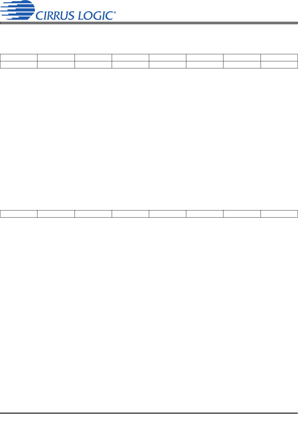
76543210
LOCKM1 LOCKM0 Reserved Reserved Reserved BSEL CAM CHS