
User guide
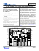
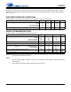
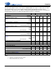
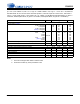
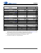
Table Of Contents
- 1. Characteristics and Specifications
- Specified Operating Conditions
- Absolute Maximum Ratings
- Analog Input Characteristics
- A/D Digital Filter Characteristics
- Analog Output Characteristics
- D/A Digital Filter Characteristics
- Switching Characteristics
- Switching Characteristics - Control Port - I²C™ Format
- Switching Characteristics - Control Port - SPI™ Format
- DC Electrical Characteristics
- Digital Interface Characteristics
- 2. Pin Descriptions
- 3. Typical Connection Diagram
- 4. Applications
- 4.1 Overview
- 4.2 Analog Inputs
- 4.3 Analog Outputs
- 4.4 S/PDIF Receiver
- 4.5 Clock Generation
- 4.6 Digital Interfaces
- 4.7 Control Port Description and Timing
- 4.8 Interrupts
- 4.9 Reset and Power-Up
- 4.10 Power Supply, Grounding, and PCB Layout
- 5. Register Quick Reference
- 6. Register Description
- Table 5. DAC De-Emphasis
- Table 6. Receiver De-Emphasis
- Table 7. Digital Interface Formats
- Table 8. ADC One-Line Mode
- Table 9. DAC One-Line Mode
- Table 10. RMCK Divider Settings
- Table 11. OMCK Frequency Settings
- Table 12. Master Clock Source Select
- Table 13. AES Format Detection
- Table 14. Receiver Clock Frequency Detection
- Table 15. Example Digital Volume Settings
- Table 16. ATAPI Decode
- Table 17. Example ADC Input Gain Settings
- Table 18. TXP Output Selection
- Table 19. Receiver Input Selection
- Table 20. Auxiliary Data Width Selection
- 7. Parameter Definitions
- 8. Appendix A: External Filters
- 9. Appendix B: S/PDIF Receiver
- 10. Appendix C: PLL Filter
- 11. Appendix D: External AES3-S/PDIF-IEC60958 Receiver Components
- 12. Appendix E: ADC Filter Plots
- Figure 34. Single-Speed Mode Stopband Rejection
- Figure 35. Single-Speed Mode Transition Band
- Figure 36. Single-Speed Mode Transition Band (Detail)
- Figure 37. Single-Speed Mode Passband Ripple
- Figure 38. Double-Speed Mode Stopband Rejection
- Figure 39. Double-Speed Mode Transition Band
- Figure 40. Double-Speed Mode Transition Band (Detail)
- Figure 41. Double-Speed Mode Passband Ripple
- Figure 42. Quad-Speed Mode Stopband Rejection
- Figure 43. Quad-Speed Mode Transition Band
- Figure 44. Quad-Speed Mode Transition Band (Detail)
- Figure 45. Quad-Speed Mode Passband Ripple
- 13. Appendix F: DAC Filter Plots
- Figure 46. Single-Speed (fast) Stopband Rejection
- Figure 47. Single-Speed (fast) Transition Band
- Figure 48. Single-Speed (fast) Transition Band (detail)
- Figure 49. Single-Speed (fast) Passband Ripple
- Figure 50. Single-Speed (slow) Stopband Rejection
- Figure 51. Single-Speed (slow) Transition Band
- Figure 52. Single-Speed (slow) Transition Band (detail)
- Figure 53. Single-Speed (slow) Passband Ripple
- Figure 54. Double-Speed (fast) Stopband Rejection
- Figure 55. Double-Speed (fast) Transition Band
- Figure 56. Double-Speed (fast) Transition Band (detail)
- Figure 57. Double-Speed (fast) Passband Ripple
- Figure 58. Double-Speed (slow) Stopband Rejection
- Figure 59. Double-Speed (slow) Transition Band
- Figure 60. Double-Speed (slow) Transition Band (detail)
- Figure 61. Double-Speed (slow) Passband Ripple
- Figure 62. Quad-Speed (fast) Stopband Rejection
- Figure 63. Quad-Speed (fast) Transition Band
- Figure 64. Quad-Speed (fast) Transition Band (detail)
- Figure 65. Quad-Speed (fast) Passband Ripple
- Figure 66. Quad-Speed (slow) Stopband Rejection
- Figure 67. Quad-Speed (slow) Transition Band
- Figure 68. Quad-Speed (slow) Transition Band (detail)
- Figure 69. Quad-Speed (slow) Passband Ripple
- 14. Package Dimensions
- 15. Ordering Information
- 16. References
- 17. Revision History
6 DS583F2
CS42516
1. CHARACTERISTICS AND SPECIFICATIONS
(All Min/Max characteristics and specifications are guaranteed over the Specified Operating Conditions. Typical
performance characteristics and specifications are derived from measurements taken at nominal supply voltages
and T
A
= 25° C.)
SPECIFIED OPERATING CONDITIONS
(AGND=DGND=0, all voltages with respect to ground; OMCK=12.288 MHz; Master Mode)
ABSOLUTE MAXIMUM RATINGS
(AGND = DGND = 0 V; all voltages with respect to ground.)
WARNING: Operation at or beyond these limits may result in permanent damage to the device. Normal operation
is not guaranteed at these extremes.
Notes:
1. Any pin except supplies. Transient currents of up to ±100 mA on the analog input pins will not cause
SCR latch-up.
2. The maximum over/under voltage is limited by the input current.
Parameter Symbol Min Typ Max Units
DC Power Supply Analog
Digital
Serial Port Interface
Control Port Interface
VA / VARX
VD
VLS
VLC
4.75
3.13
1.8
1.8
5.0
3.3
5.0
5.0
5.25
5.25
5.25
5.25
V
V
V
V
Ambient Operating Temperature (power applied)
T
A
-10 - +70 C
Parameters Symbol Min Max Units
DC Power Supply Analog
Digital
Serial Port Interface
Control Port Interface
VA / VARX
VD
VLS
VLC
-0.3
-0.3
-0.3
-0.3
6.0
6.0
6.0
6.0
V
V
V
V
Input Current (Note 1)
I
in
-±10mA
Analog Input Voltage (Note 2)
V
IN
AGND-0.7 VA+0.7 V
Digital Input Voltage Serial Port Interface
(Note 2) Control Port Interface
S/PDIF interface
V
IND-S
V
IND-C
V
IND-SP
-0.3
-0.3
-0.3
VLS+ 0.4
VLC+ 0.4
VARX+0.4
V
V
V
Ambient Operating Temperature(power applied)
T
A
T
A
-20
-50
+85
+95
°C
°C
Storage Temperature
T
stg
-65 +150 °C