
User guide
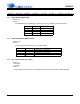
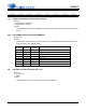
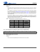
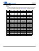
Table Of Contents
- 1. Characteristics and Specifications
- Specified Operating Conditions
- Absolute Maximum Ratings
- Analog Input Characteristics
- A/D Digital Filter Characteristics
- Analog Output Characteristics
- D/A Digital Filter Characteristics
- Switching Characteristics
- Switching Characteristics - Control Port - I²C™ Format
- Switching Characteristics - Control Port - SPI™ Format
- DC Electrical Characteristics
- Digital Interface Characteristics
- 2. Pin Descriptions
- 3. Typical Connection Diagram
- 4. Applications
- 4.1 Overview
- 4.2 Analog Inputs
- 4.3 Analog Outputs
- 4.4 S/PDIF Receiver
- 4.5 Clock Generation
- 4.6 Digital Interfaces
- 4.7 Control Port Description and Timing
- 4.8 Interrupts
- 4.9 Reset and Power-Up
- 4.10 Power Supply, Grounding, and PCB Layout
- 5. Register Quick Reference
- 6. Register Description
- Table 5. DAC De-Emphasis
- Table 6. Receiver De-Emphasis
- Table 7. Digital Interface Formats
- Table 8. ADC One-Line Mode
- Table 9. DAC One-Line Mode
- Table 10. RMCK Divider Settings
- Table 11. OMCK Frequency Settings
- Table 12. Master Clock Source Select
- Table 13. AES Format Detection
- Table 14. Receiver Clock Frequency Detection
- Table 15. Example Digital Volume Settings
- Table 16. ATAPI Decode
- Table 17. Example ADC Input Gain Settings
- Table 18. TXP Output Selection
- Table 19. Receiver Input Selection
- Table 20. Auxiliary Data Width Selection
- 7. Parameter Definitions
- 8. Appendix A: External Filters
- 9. Appendix B: S/PDIF Receiver
- 10. Appendix C: PLL Filter
- 11. Appendix D: External AES3-S/PDIF-IEC60958 Receiver Components
- 12. Appendix E: ADC Filter Plots
- Figure 34. Single-Speed Mode Stopband Rejection
- Figure 35. Single-Speed Mode Transition Band
- Figure 36. Single-Speed Mode Transition Band (Detail)
- Figure 37. Single-Speed Mode Passband Ripple
- Figure 38. Double-Speed Mode Stopband Rejection
- Figure 39. Double-Speed Mode Transition Band
- Figure 40. Double-Speed Mode Transition Band (Detail)
- Figure 41. Double-Speed Mode Passband Ripple
- Figure 42. Quad-Speed Mode Stopband Rejection
- Figure 43. Quad-Speed Mode Transition Band
- Figure 44. Quad-Speed Mode Transition Band (Detail)
- Figure 45. Quad-Speed Mode Passband Ripple
- 13. Appendix F: DAC Filter Plots
- Figure 46. Single-Speed (fast) Stopband Rejection
- Figure 47. Single-Speed (fast) Transition Band
- Figure 48. Single-Speed (fast) Transition Band (detail)
- Figure 49. Single-Speed (fast) Passband Ripple
- Figure 50. Single-Speed (slow) Stopband Rejection
- Figure 51. Single-Speed (slow) Transition Band
- Figure 52. Single-Speed (slow) Transition Band (detail)
- Figure 53. Single-Speed (slow) Passband Ripple
- Figure 54. Double-Speed (fast) Stopband Rejection
- Figure 55. Double-Speed (fast) Transition Band
- Figure 56. Double-Speed (fast) Transition Band (detail)
- Figure 57. Double-Speed (fast) Passband Ripple
- Figure 58. Double-Speed (slow) Stopband Rejection
- Figure 59. Double-Speed (slow) Transition Band
- Figure 60. Double-Speed (slow) Transition Band (detail)
- Figure 61. Double-Speed (slow) Passband Ripple
- Figure 62. Quad-Speed (fast) Stopband Rejection
- Figure 63. Quad-Speed (fast) Transition Band
- Figure 64. Quad-Speed (fast) Transition Band (detail)
- Figure 65. Quad-Speed (fast) Passband Ripple
- Figure 66. Quad-Speed (slow) Stopband Rejection
- Figure 67. Quad-Speed (slow) Transition Band
- Figure 68. Quad-Speed (slow) Transition Band (detail)
- Figure 69. Quad-Speed (slow) Passband Ripple
- 14. Package Dimensions
- 15. Ordering Information
- 16. References
- 17. Revision History

DS583F2 55
CS42516
6.9.4 RECEIVER CLOCK FREQUENCY (RCVR_CLKX)
Default = xxx
Function:
The CS42516 detects the ratio between the OMCK and the recovered clock from the PLL. Given the
absolute frequency of OMCK, this ratio may be used to determine the absolute frequency of the PLL
clock.
If a 12.2880 MHz, 18.4320 MHz, or 24.5760 MHz clock is applied to OMCK and the OMCK_FREQX
bits are set accordingly (see “OMCK Frequency (OMCK Freqx)” on page 52), the absolute frequency
of the PLL clock is reflected in the RCVR_CLKX bits according to Table 16. If the absolute frequency
of the PLL clock does not match one of the frequencies given in Table 16, these bits will reflect the
closest available value.
If the frequency of OMCK is not equal to 12.2880 MHz, 18.4320 MHz, or 24.5760 MHz, the contents
of the RCVR_CLKX bits will be inaccurate and should be disregarded. In this case, an external con-
troller may use the contents of the OMCK/PLL_CLK ratio register and the known OMCK frequency to
determine the absolute frequency of the PLL clock.
Note: These bits are set to ‘111’b when the FRC_PLL_LK bit is ‘1’b.
6.10 Burst Preamble PC and PD Bytes (addresses 09h - 0Ch)(Read Only)
6.10.1 BURST PREAMBLE BITS (PCX & PDX)
Default = xxh
Function:
The PC and PD burst preamble bytes are loaded into these four registers.
RCVR_CLK2 RCVR_CLK1 RCVR_CLK0 Description
0 0 0 8.1920 MHz
0 0 1 11.2896 MHz
0 1 0 12.288 MHz
0 1 1 16.3840 MHz
1 0 0 22.5792 MHz
1 0 1 24.5760 MHz
1 1 0 45.1584 MHz
1 1 1 49.1520 MHz
Table 14. Receiver Clock Frequency Detection
76543210
PCx-7 PCx-6 PCx-5 PCx-4 PCx-3 PCx-2 PCx-1 PCx-0
PDx-7 PDx-6 PDx-5 PDx-4 PDx-3 PDx-2 PDx-1 PDx-0