
User guide
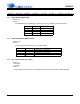
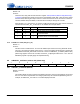
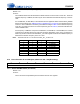
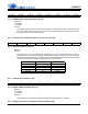
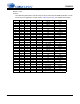
Table Of Contents
- 1. Characteristics and Specifications
- Specified Operating Conditions
- Absolute Maximum Ratings
- Analog Input Characteristics
- A/D Digital Filter Characteristics
- Analog Output Characteristics
- D/A Digital Filter Characteristics
- Switching Characteristics
- Switching Characteristics - Control Port - I²C™ Format
- Switching Characteristics - Control Port - SPI™ Format
- DC Electrical Characteristics
- Digital Interface Characteristics
- 2. Pin Descriptions
- 3. Typical Connection Diagram
- 4. Applications
- 4.1 Overview
- 4.2 Analog Inputs
- 4.3 Analog Outputs
- 4.4 S/PDIF Receiver
- 4.5 Clock Generation
- 4.6 Digital Interfaces
- 4.7 Control Port Description and Timing
- 4.8 Interrupts
- 4.9 Reset and Power-Up
- 4.10 Power Supply, Grounding, and PCB Layout
- 5. Register Quick Reference
- 6. Register Description
- Table 5. DAC De-Emphasis
- Table 6. Receiver De-Emphasis
- Table 7. Digital Interface Formats
- Table 8. ADC One-Line Mode
- Table 9. DAC One-Line Mode
- Table 10. RMCK Divider Settings
- Table 11. OMCK Frequency Settings
- Table 12. Master Clock Source Select
- Table 13. AES Format Detection
- Table 14. Receiver Clock Frequency Detection
- Table 15. Example Digital Volume Settings
- Table 16. ATAPI Decode
- Table 17. Example ADC Input Gain Settings
- Table 18. TXP Output Selection
- Table 19. Receiver Input Selection
- Table 20. Auxiliary Data Width Selection
- 7. Parameter Definitions
- 8. Appendix A: External Filters
- 9. Appendix B: S/PDIF Receiver
- 10. Appendix C: PLL Filter
- 11. Appendix D: External AES3-S/PDIF-IEC60958 Receiver Components
- 12. Appendix E: ADC Filter Plots
- Figure 34. Single-Speed Mode Stopband Rejection
- Figure 35. Single-Speed Mode Transition Band
- Figure 36. Single-Speed Mode Transition Band (Detail)
- Figure 37. Single-Speed Mode Passband Ripple
- Figure 38. Double-Speed Mode Stopband Rejection
- Figure 39. Double-Speed Mode Transition Band
- Figure 40. Double-Speed Mode Transition Band (Detail)
- Figure 41. Double-Speed Mode Passband Ripple
- Figure 42. Quad-Speed Mode Stopband Rejection
- Figure 43. Quad-Speed Mode Transition Band
- Figure 44. Quad-Speed Mode Transition Band (Detail)
- Figure 45. Quad-Speed Mode Passband Ripple
- 13. Appendix F: DAC Filter Plots
- Figure 46. Single-Speed (fast) Stopband Rejection
- Figure 47. Single-Speed (fast) Transition Band
- Figure 48. Single-Speed (fast) Transition Band (detail)
- Figure 49. Single-Speed (fast) Passband Ripple
- Figure 50. Single-Speed (slow) Stopband Rejection
- Figure 51. Single-Speed (slow) Transition Band
- Figure 52. Single-Speed (slow) Transition Band (detail)
- Figure 53. Single-Speed (slow) Passband Ripple
- Figure 54. Double-Speed (fast) Stopband Rejection
- Figure 55. Double-Speed (fast) Transition Band
- Figure 56. Double-Speed (fast) Transition Band (detail)
- Figure 57. Double-Speed (fast) Passband Ripple
- Figure 58. Double-Speed (slow) Stopband Rejection
- Figure 59. Double-Speed (slow) Transition Band
- Figure 60. Double-Speed (slow) Transition Band (detail)
- Figure 61. Double-Speed (slow) Passband Ripple
- Figure 62. Quad-Speed (fast) Stopband Rejection
- Figure 63. Quad-Speed (fast) Transition Band
- Figure 64. Quad-Speed (fast) Transition Band (detail)
- Figure 65. Quad-Speed (fast) Passband Ripple
- Figure 66. Quad-Speed (slow) Stopband Rejection
- Figure 67. Quad-Speed (slow) Transition Band
- Figure 68. Quad-Speed (slow) Transition Band (detail)
- Figure 69. Quad-Speed (slow) Passband Ripple
- 14. Package Dimensions
- 15. Ordering Information
- 16. References
- 17. Revision History
DS583F2 53
CS42516
6.7.4 MASTER CLOCK SOURCE SELECT (SW_CTRLX)
Default = 00
Function:
These two bits, along with the UNLOCK bit in register “Interrupt Status (address 20h) (Read Only)”
on page 63, determine the master clock source for the CS42516. When SW_CTRL1 and SW_CTRL0
are set to '00'b, selecting the output of the PLL as the internal clock source, and the PLL becomes
unlocked, RMCK will equal OMCK, but all internal and serial port timings are not valid.
When the FRC_PLL_LK bit is set to ‘1’b, the SW_CTRLX bits must be set to ‘00’b. If the PLL becomes
unlocked when the FRC_PLL_LK bit is set to ‘1’b, RMCK will not equal OMCK.
6.7.5 FORCE PLL LOCK (FRC_PLL_LK)
Default = 0
Function:
This bit is used to enable the PLL to lock to the S/PDIF input stream or the SAI_LRCK with the ab-
sence of a clock signal on OMCK. When set to a ‘1’b, the auto-detect sample frequency feature will
be disabled and the SW_CTRLX bits must be set to ‘00’b. The OMCK/PLL_CLK Ratio (address 07h)
(Read Only) register contents are not valid, and the PLL_CLK[2:0] bits will be set to ‘111’b. Use the
DE-EMPH[1:0] bits to properly apply de-emphasis filtering.
6.8 OMCK/PLL_CLK Ratio (address 07h) (Read Only)
6.8.1 OMCK/PLL_CLK RATIO (RATIOX)
Default = xxxxxxxx
Function:
This register allows the user to find the exact absolute frequency of the recovered MCLK coming from
the PLL. This value is represented as an integer (RATIO7:6) and a fractional (RATIO5:0) part. For
example, an OMCK/PLL_CLK ratio of 1.5 would be displayed as 60h.
SW_CTRL1 SW_CTRL0 UNLOCK Description
0 0 X Manual setting, MCLK sourced from PLL.
0 1 X Manual setting, MCLK sourced from OMCK.
10
0
1
Hold, keep same MCLK source.Auto switch, MCLK
sourced from OMCK.
11
0
1
Auto switch, MCLK sourced from PLL.
Auto switch, MCLK sourced from OMCK.
Table 12. Master Clock Source Select
76543210
RATIO7(2
1
)RATIO6(2
0
)RATIO5(2
-1
)RATIO4(2
-2
)RATIO3(2
-3
)RATIO2(2
-4
)RATIO1(2
-5
)RATIO0(2
-6
)