
User guide
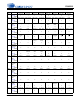
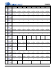
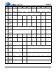
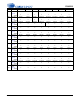
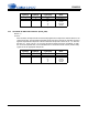
Table Of Contents
- 1. Characteristics and Specifications
- Specified Operating Conditions
- Absolute Maximum Ratings
- Analog Input Characteristics
- A/D Digital Filter Characteristics
- Analog Output Characteristics
- D/A Digital Filter Characteristics
- Switching Characteristics
- Switching Characteristics - Control Port - I²C™ Format
- Switching Characteristics - Control Port - SPI™ Format
- DC Electrical Characteristics
- Digital Interface Characteristics
- 2. Pin Descriptions
- 3. Typical Connection Diagram
- 4. Applications
- 4.1 Overview
- 4.2 Analog Inputs
- 4.3 Analog Outputs
- 4.4 S/PDIF Receiver
- 4.5 Clock Generation
- 4.6 Digital Interfaces
- 4.7 Control Port Description and Timing
- 4.8 Interrupts
- 4.9 Reset and Power-Up
- 4.10 Power Supply, Grounding, and PCB Layout
- 5. Register Quick Reference
- 6. Register Description
- Table 5. DAC De-Emphasis
- Table 6. Receiver De-Emphasis
- Table 7. Digital Interface Formats
- Table 8. ADC One-Line Mode
- Table 9. DAC One-Line Mode
- Table 10. RMCK Divider Settings
- Table 11. OMCK Frequency Settings
- Table 12. Master Clock Source Select
- Table 13. AES Format Detection
- Table 14. Receiver Clock Frequency Detection
- Table 15. Example Digital Volume Settings
- Table 16. ATAPI Decode
- Table 17. Example ADC Input Gain Settings
- Table 18. TXP Output Selection
- Table 19. Receiver Input Selection
- Table 20. Auxiliary Data Width Selection
- 7. Parameter Definitions
- 8. Appendix A: External Filters
- 9. Appendix B: S/PDIF Receiver
- 10. Appendix C: PLL Filter
- 11. Appendix D: External AES3-S/PDIF-IEC60958 Receiver Components
- 12. Appendix E: ADC Filter Plots
- Figure 34. Single-Speed Mode Stopband Rejection
- Figure 35. Single-Speed Mode Transition Band
- Figure 36. Single-Speed Mode Transition Band (Detail)
- Figure 37. Single-Speed Mode Passband Ripple
- Figure 38. Double-Speed Mode Stopband Rejection
- Figure 39. Double-Speed Mode Transition Band
- Figure 40. Double-Speed Mode Transition Band (Detail)
- Figure 41. Double-Speed Mode Passband Ripple
- Figure 42. Quad-Speed Mode Stopband Rejection
- Figure 43. Quad-Speed Mode Transition Band
- Figure 44. Quad-Speed Mode Transition Band (Detail)
- Figure 45. Quad-Speed Mode Passband Ripple
- 13. Appendix F: DAC Filter Plots
- Figure 46. Single-Speed (fast) Stopband Rejection
- Figure 47. Single-Speed (fast) Transition Band
- Figure 48. Single-Speed (fast) Transition Band (detail)
- Figure 49. Single-Speed (fast) Passband Ripple
- Figure 50. Single-Speed (slow) Stopband Rejection
- Figure 51. Single-Speed (slow) Transition Band
- Figure 52. Single-Speed (slow) Transition Band (detail)
- Figure 53. Single-Speed (slow) Passband Ripple
- Figure 54. Double-Speed (fast) Stopband Rejection
- Figure 55. Double-Speed (fast) Transition Band
- Figure 56. Double-Speed (fast) Transition Band (detail)
- Figure 57. Double-Speed (fast) Passband Ripple
- Figure 58. Double-Speed (slow) Stopband Rejection
- Figure 59. Double-Speed (slow) Transition Band
- Figure 60. Double-Speed (slow) Transition Band (detail)
- Figure 61. Double-Speed (slow) Passband Ripple
- Figure 62. Quad-Speed (fast) Stopband Rejection
- Figure 63. Quad-Speed (fast) Transition Band
- Figure 64. Quad-Speed (fast) Transition Band (detail)
- Figure 65. Quad-Speed (fast) Passband Ripple
- Figure 66. Quad-Speed (slow) Stopband Rejection
- Figure 67. Quad-Speed (slow) Transition Band
- Figure 68. Quad-Speed (slow) Transition Band (detail)
- Figure 69. Quad-Speed (slow) Passband Ripple
- 14. Package Dimensions
- 15. Ordering Information
- 16. References
- 17. Revision History
50 DS583F2
CS42516
6.5.4 SAI RIGHT-JUSTIFIED BITS (SAI_RJ16)
Default = 0
Function:
This bit determines how many bits to use during right-justified mode for the Serial Audio Interface
Port. By default the receiver will be in RJ24 bits but can be set to RJ16 bits.
0 - 24 bit mode.
1 - 16 bit mode.
6.5.5 CODEC RIGHT-JUSTIFIED BITS (CODEC_RJ16)
Default = 0
Function:
This bit determines how many bits to use during Right-Justified Mode for the DAC and ADC within
the CODEC Serial Port. By default, the DAC and ADC will be in RJ24 bits, but can be set to RJ16 bits.
0 - 24 bit mode.
1 - 16 bit mode.
6.6 Misc Control (address 05h)
6.6.1 EXTERNAL ADC SCLK SELECT (EXT ADC SCLK)
Default = 0
Function:
This bit identifies the SCLK source for the external ADCs attached to the ADCIN1/2 ports when using
One-Line Mode of operation.
0 - SAI_SCLK is used as external ADC SCLK.
1 - CX_SCLK is used as external ADC SCLK.
6.6.2 RMCK HIGH IMPEDANCE (HIZ_RMCK)
Default = 0
Function:
This bit is used to create a high-impedance output on RMCK when the clock signal is not required.
6.6.3 FREEZE CONTROLS (FREEZE)
Default = 0
Function:
This function will freeze the previous output of, and allow modifications to be made to, the Volume
Control (address 0Fh-16h), Channel Invert (address 17h), and Mixing Control Pair (address 18h-1Bh)
registers without the changes taking effect until the FREEZE is disabled. To make multiple changes
in these control port registers take effect simultaneously, enable the FREEZE bit, make all register
changes, then disable the FREEZE bit.
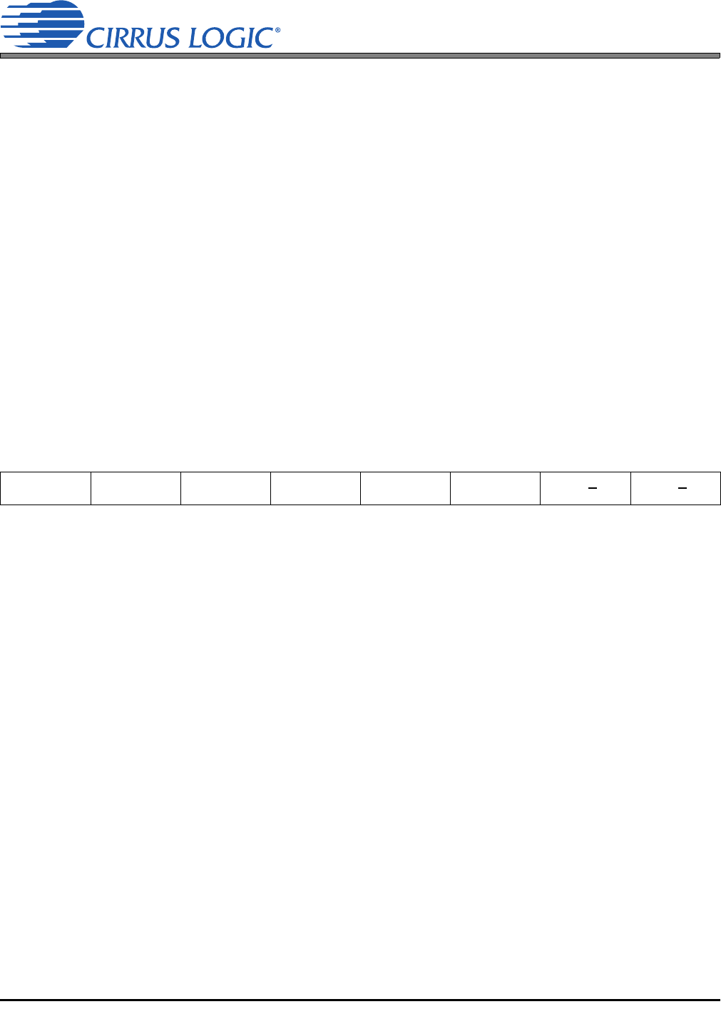
76543210
Ext ADC SCLK HiZ_RMCK Reserved FREEZE FILT_SEL HPF_FREEZE CODEC_SP
M/S
SAI_SP
M/S