
User guide
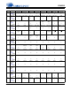
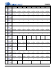
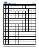
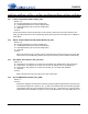
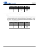
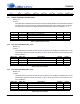
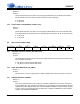
Table Of Contents
- 1. Characteristics and Specifications
- Specified Operating Conditions
- Absolute Maximum Ratings
- Analog Input Characteristics
- A/D Digital Filter Characteristics
- Analog Output Characteristics
- D/A Digital Filter Characteristics
- Switching Characteristics
- Switching Characteristics - Control Port - I²C™ Format
- Switching Characteristics - Control Port - SPI™ Format
- DC Electrical Characteristics
- Digital Interface Characteristics
- 2. Pin Descriptions
- 3. Typical Connection Diagram
- 4. Applications
- 4.1 Overview
- 4.2 Analog Inputs
- 4.3 Analog Outputs
- 4.4 S/PDIF Receiver
- 4.5 Clock Generation
- 4.6 Digital Interfaces
- 4.7 Control Port Description and Timing
- 4.8 Interrupts
- 4.9 Reset and Power-Up
- 4.10 Power Supply, Grounding, and PCB Layout
- 5. Register Quick Reference
- 6. Register Description
- Table 5. DAC De-Emphasis
- Table 6. Receiver De-Emphasis
- Table 7. Digital Interface Formats
- Table 8. ADC One-Line Mode
- Table 9. DAC One-Line Mode
- Table 10. RMCK Divider Settings
- Table 11. OMCK Frequency Settings
- Table 12. Master Clock Source Select
- Table 13. AES Format Detection
- Table 14. Receiver Clock Frequency Detection
- Table 15. Example Digital Volume Settings
- Table 16. ATAPI Decode
- Table 17. Example ADC Input Gain Settings
- Table 18. TXP Output Selection
- Table 19. Receiver Input Selection
- Table 20. Auxiliary Data Width Selection
- 7. Parameter Definitions
- 8. Appendix A: External Filters
- 9. Appendix B: S/PDIF Receiver
- 10. Appendix C: PLL Filter
- 11. Appendix D: External AES3-S/PDIF-IEC60958 Receiver Components
- 12. Appendix E: ADC Filter Plots
- Figure 34. Single-Speed Mode Stopband Rejection
- Figure 35. Single-Speed Mode Transition Band
- Figure 36. Single-Speed Mode Transition Band (Detail)
- Figure 37. Single-Speed Mode Passband Ripple
- Figure 38. Double-Speed Mode Stopband Rejection
- Figure 39. Double-Speed Mode Transition Band
- Figure 40. Double-Speed Mode Transition Band (Detail)
- Figure 41. Double-Speed Mode Passband Ripple
- Figure 42. Quad-Speed Mode Stopband Rejection
- Figure 43. Quad-Speed Mode Transition Band
- Figure 44. Quad-Speed Mode Transition Band (Detail)
- Figure 45. Quad-Speed Mode Passband Ripple
- 13. Appendix F: DAC Filter Plots
- Figure 46. Single-Speed (fast) Stopband Rejection
- Figure 47. Single-Speed (fast) Transition Band
- Figure 48. Single-Speed (fast) Transition Band (detail)
- Figure 49. Single-Speed (fast) Passband Ripple
- Figure 50. Single-Speed (slow) Stopband Rejection
- Figure 51. Single-Speed (slow) Transition Band
- Figure 52. Single-Speed (slow) Transition Band (detail)
- Figure 53. Single-Speed (slow) Passband Ripple
- Figure 54. Double-Speed (fast) Stopband Rejection
- Figure 55. Double-Speed (fast) Transition Band
- Figure 56. Double-Speed (fast) Transition Band (detail)
- Figure 57. Double-Speed (fast) Passband Ripple
- Figure 58. Double-Speed (slow) Stopband Rejection
- Figure 59. Double-Speed (slow) Transition Band
- Figure 60. Double-Speed (slow) Transition Band (detail)
- Figure 61. Double-Speed (slow) Passband Ripple
- Figure 62. Quad-Speed (fast) Stopband Rejection
- Figure 63. Quad-Speed (fast) Transition Band
- Figure 64. Quad-Speed (fast) Transition Band (detail)
- Figure 65. Quad-Speed (fast) Passband Ripple
- Figure 66. Quad-Speed (slow) Stopband Rejection
- Figure 67. Quad-Speed (slow) Transition Band
- Figure 68. Quad-Speed (slow) Transition Band (detail)
- Figure 69. Quad-Speed (slow) Passband Ripple
- 14. Package Dimensions
- 15. Ordering Information
- 16. References
- 17. Revision History
DS583F2 45
CS42516
6. REGISTER DESCRIPTION
All registers are read/write except for the I.D. and Revision Register, OMCK/PLL_CLK Ratio Register, Interrupt Sta-
tus Register, and Q-Channel Subcode Bytes and C-bit or U-bit Data Buffer, which are read only. See the following
bit definition tables for bit assignment information. The default state of each bit after a power-up sequence or reset
is listed in each bit description.
6.1 Memory Address Pointer (MAP)
Not a register
6.1.1 INCREMENT (INCR)
Default = 1
Function:
Memory Address Pointer auto increment control
0 - MAP is not incremented automatically.
1 - Internal MAP is automatically incremented after each read or write.
6.1.2 MEMORY ADDRESS POINTER (MAPX)
Default = 0000001
Function:
Memory Address Pointer (MAP). Sets the register address that will be read or written by the control
port.
6.2 Chip I.D. and Revision Register (address 01h) (Read Only)
6.2.1 CHIP I.D. (CHIP_IDX)
Default = 1110
Function:
I.D. code for the CS42516. Permanently set to 1110.
6.2.2 CHIP REVISION (REV_IDX)
Default = xxxx
Function:
CS42516 revision level.
Revision D is coded as 0100.
Revision C is coded as 0011.
76543210
INCR MAP6 MAP5 MAP4 MAP3 MAP2 MAP1 MAP0
76543210
Chip_ID3 Chip_ID2 Chip_ID1 CHIP_ID0 Rev_ID3 Rev_ID2 Rev_ID1 Rev_ID0