
User guide
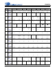
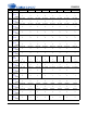
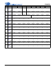
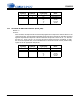
Table Of Contents
- 1. Characteristics and Specifications
- Specified Operating Conditions
- Absolute Maximum Ratings
- Analog Input Characteristics
- A/D Digital Filter Characteristics
- Analog Output Characteristics
- D/A Digital Filter Characteristics
- Switching Characteristics
- Switching Characteristics - Control Port - I²C™ Format
- Switching Characteristics - Control Port - SPI™ Format
- DC Electrical Characteristics
- Digital Interface Characteristics
- 2. Pin Descriptions
- 3. Typical Connection Diagram
- 4. Applications
- 4.1 Overview
- 4.2 Analog Inputs
- 4.3 Analog Outputs
- 4.4 S/PDIF Receiver
- 4.5 Clock Generation
- 4.6 Digital Interfaces
- 4.7 Control Port Description and Timing
- 4.8 Interrupts
- 4.9 Reset and Power-Up
- 4.10 Power Supply, Grounding, and PCB Layout
- 5. Register Quick Reference
- 6. Register Description
- Table 5. DAC De-Emphasis
- Table 6. Receiver De-Emphasis
- Table 7. Digital Interface Formats
- Table 8. ADC One-Line Mode
- Table 9. DAC One-Line Mode
- Table 10. RMCK Divider Settings
- Table 11. OMCK Frequency Settings
- Table 12. Master Clock Source Select
- Table 13. AES Format Detection
- Table 14. Receiver Clock Frequency Detection
- Table 15. Example Digital Volume Settings
- Table 16. ATAPI Decode
- Table 17. Example ADC Input Gain Settings
- Table 18. TXP Output Selection
- Table 19. Receiver Input Selection
- Table 20. Auxiliary Data Width Selection
- 7. Parameter Definitions
- 8. Appendix A: External Filters
- 9. Appendix B: S/PDIF Receiver
- 10. Appendix C: PLL Filter
- 11. Appendix D: External AES3-S/PDIF-IEC60958 Receiver Components
- 12. Appendix E: ADC Filter Plots
- Figure 34. Single-Speed Mode Stopband Rejection
- Figure 35. Single-Speed Mode Transition Band
- Figure 36. Single-Speed Mode Transition Band (Detail)
- Figure 37. Single-Speed Mode Passband Ripple
- Figure 38. Double-Speed Mode Stopband Rejection
- Figure 39. Double-Speed Mode Transition Band
- Figure 40. Double-Speed Mode Transition Band (Detail)
- Figure 41. Double-Speed Mode Passband Ripple
- Figure 42. Quad-Speed Mode Stopband Rejection
- Figure 43. Quad-Speed Mode Transition Band
- Figure 44. Quad-Speed Mode Transition Band (Detail)
- Figure 45. Quad-Speed Mode Passband Ripple
- 13. Appendix F: DAC Filter Plots
- Figure 46. Single-Speed (fast) Stopband Rejection
- Figure 47. Single-Speed (fast) Transition Band
- Figure 48. Single-Speed (fast) Transition Band (detail)
- Figure 49. Single-Speed (fast) Passband Ripple
- Figure 50. Single-Speed (slow) Stopband Rejection
- Figure 51. Single-Speed (slow) Transition Band
- Figure 52. Single-Speed (slow) Transition Band (detail)
- Figure 53. Single-Speed (slow) Passband Ripple
- Figure 54. Double-Speed (fast) Stopband Rejection
- Figure 55. Double-Speed (fast) Transition Band
- Figure 56. Double-Speed (fast) Transition Band (detail)
- Figure 57. Double-Speed (fast) Passband Ripple
- Figure 58. Double-Speed (slow) Stopband Rejection
- Figure 59. Double-Speed (slow) Transition Band
- Figure 60. Double-Speed (slow) Transition Band (detail)
- Figure 61. Double-Speed (slow) Passband Ripple
- Figure 62. Quad-Speed (fast) Stopband Rejection
- Figure 63. Quad-Speed (fast) Transition Band
- Figure 64. Quad-Speed (fast) Transition Band (detail)
- Figure 65. Quad-Speed (fast) Passband Ripple
- Figure 66. Quad-Speed (slow) Stopband Rejection
- Figure 67. Quad-Speed (slow) Transition Band
- Figure 68. Quad-Speed (slow) Transition Band (detail)
- Figure 69. Quad-Speed (slow) Passband Ripple
- 14. Package Dimensions
- 15. Ordering Information
- 16. References
- 17. Revision History
DS583F2 41
CS42516
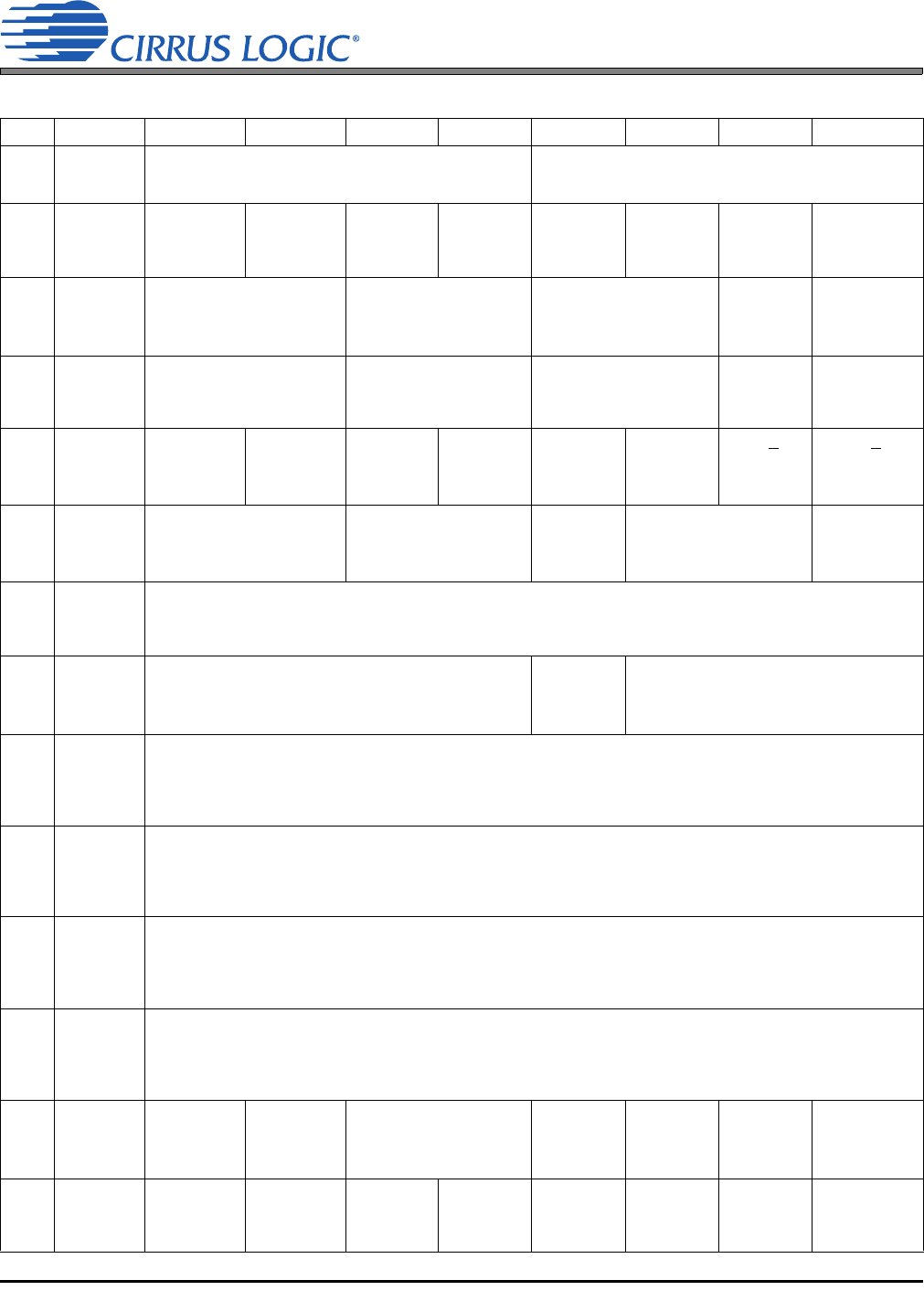
5. REGISTER QUICK REFERENCE
Addr Function 7 6 5 4 3 2 1 0
01h
ID
Chip_ID3 Chip_ID2 Chip_ID1 Chip_ID0 Rev_ID3 Rev_ID2 Rev_ID1 Rev_ID0
page 45
default
1110XXXX
02h
Power Con-
trol
PDN_RCVR1 PDN_RCVR0 PDN_ADC Reserved PDN_DAC3 PDN_DAC2 PDN_DAC1 PDN
page 46
default
1 0 00000 1
03h
Functional
Mode
CODEC_FM1 CODEC_FM0 SAI_FM1 SAI_FM0 ADC_SP
SEL1
ADC_SP
SEL0
DAC_DEM RCVR_DEM
page 45
default
0 0 00000 0
04h
Interface
Formats
DIF1 DIF0 ADC_OL1 ADC_OL0 DAC_OL1 DAC_OL0 SAI_RJ16 CODEC_RJ16
page 49
default
0 1 00000 0
05h
Misc Control
Ext ADC
SCLK
HiZ_RMCK Reserved FREEZE FILTSEL HPF_
FREEZE
CODEC_SP
M/S
SAI_SP
M/S
page 50
default
0 0 00000 0
06h
Clock Con-
trol
RMCK_DIV1 RMCK_DIV0 OMCK
Freq1
OMCK
Freq0
PLL_LRCK SW_CTRL1 SW_CTRL0 FRC_PLL_LK
page 52
default
0 0 00000 0
07h
OMCK/PLL_
CLK Ratio
RATIO7 RATIO6 RATIO5 RATIO4 RATIO3 RATIO2 RATIO1 RATIO0
page 53
default
XXXXXXX X
08h
RVCR Sta-
tus
Digital Silence AES
Format2
AES For-
mat1
AES For-
mat0
Active_CLK RVCR_CLK2 RVCR_CLK1 RVCR_CLK0
page 54
default
XXXXXXX X
09h
Burst Pre-
amble PC
Byte 0
PC0-7 PC0-6 PC0-5 PC0-4 PC0-3 PC0-2 PC0-1 PC0-0
page 55
default
XXXXXXX X
0Ah
Burst Pre-
amble PC
Byte 1
PC1-7 PC1-6 PC1-5 PC1-4 PC1-3 PC1-2 PC1-1 PC1-0
page 55
default
XXXXXXX X
0Bh
Burst Pre-
amble PD
Byte 0
PD0-7 PD0-6 PD0-5 PD0-4 PD0-3 PD0-2 PD0-1 PD0-0
page 55
default
XXXXXXX X
0Ch
Burst Pre-
amble PD
Byte 1
PD1-7 PD1-6 PD1-5 PD1-4 PD1-3 PD1-2 PD1-1 PD1-0
page 55
default
XXXXXXX X
0Dh
Volume
Control
Reserved SNGVOL SZC1 SZC0 AMUTE MUTE
SAI_SP
RAMP_UP RAMP_DN
page 56
default
0 0 00100 0
0Eh
Channel
Mute
Reserved Reserved B3_MUTE A3_MUTE B2_MUTE A2_MUTE B1_MUTE A1_MUTE
page 58
default
0 0 00000 0