
User guide
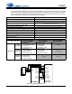
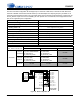
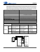
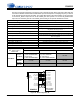
Table Of Contents
- 1. Characteristics and Specifications
- Specified Operating Conditions
- Absolute Maximum Ratings
- Analog Input Characteristics
- A/D Digital Filter Characteristics
- Analog Output Characteristics
- D/A Digital Filter Characteristics
- Switching Characteristics
- Switching Characteristics - Control Port - I²C™ Format
- Switching Characteristics - Control Port - SPI™ Format
- DC Electrical Characteristics
- Digital Interface Characteristics
- 2. Pin Descriptions
- 3. Typical Connection Diagram
- 4. Applications
- 4.1 Overview
- 4.2 Analog Inputs
- 4.3 Analog Outputs
- 4.4 S/PDIF Receiver
- 4.5 Clock Generation
- 4.6 Digital Interfaces
- 4.7 Control Port Description and Timing
- 4.8 Interrupts
- 4.9 Reset and Power-Up
- 4.10 Power Supply, Grounding, and PCB Layout
- 5. Register Quick Reference
- 6. Register Description
- Table 5. DAC De-Emphasis
- Table 6. Receiver De-Emphasis
- Table 7. Digital Interface Formats
- Table 8. ADC One-Line Mode
- Table 9. DAC One-Line Mode
- Table 10. RMCK Divider Settings
- Table 11. OMCK Frequency Settings
- Table 12. Master Clock Source Select
- Table 13. AES Format Detection
- Table 14. Receiver Clock Frequency Detection
- Table 15. Example Digital Volume Settings
- Table 16. ATAPI Decode
- Table 17. Example ADC Input Gain Settings
- Table 18. TXP Output Selection
- Table 19. Receiver Input Selection
- Table 20. Auxiliary Data Width Selection
- 7. Parameter Definitions
- 8. Appendix A: External Filters
- 9. Appendix B: S/PDIF Receiver
- 10. Appendix C: PLL Filter
- 11. Appendix D: External AES3-S/PDIF-IEC60958 Receiver Components
- 12. Appendix E: ADC Filter Plots
- Figure 34. Single-Speed Mode Stopband Rejection
- Figure 35. Single-Speed Mode Transition Band
- Figure 36. Single-Speed Mode Transition Band (Detail)
- Figure 37. Single-Speed Mode Passband Ripple
- Figure 38. Double-Speed Mode Stopband Rejection
- Figure 39. Double-Speed Mode Transition Band
- Figure 40. Double-Speed Mode Transition Band (Detail)
- Figure 41. Double-Speed Mode Passband Ripple
- Figure 42. Quad-Speed Mode Stopband Rejection
- Figure 43. Quad-Speed Mode Transition Band
- Figure 44. Quad-Speed Mode Transition Band (Detail)
- Figure 45. Quad-Speed Mode Passband Ripple
- 13. Appendix F: DAC Filter Plots
- Figure 46. Single-Speed (fast) Stopband Rejection
- Figure 47. Single-Speed (fast) Transition Band
- Figure 48. Single-Speed (fast) Transition Band (detail)
- Figure 49. Single-Speed (fast) Passband Ripple
- Figure 50. Single-Speed (slow) Stopband Rejection
- Figure 51. Single-Speed (slow) Transition Band
- Figure 52. Single-Speed (slow) Transition Band (detail)
- Figure 53. Single-Speed (slow) Passband Ripple
- Figure 54. Double-Speed (fast) Stopband Rejection
- Figure 55. Double-Speed (fast) Transition Band
- Figure 56. Double-Speed (fast) Transition Band (detail)
- Figure 57. Double-Speed (fast) Passband Ripple
- Figure 58. Double-Speed (slow) Stopband Rejection
- Figure 59. Double-Speed (slow) Transition Band
- Figure 60. Double-Speed (slow) Transition Band (detail)
- Figure 61. Double-Speed (slow) Passband Ripple
- Figure 62. Quad-Speed (fast) Stopband Rejection
- Figure 63. Quad-Speed (fast) Transition Band
- Figure 64. Quad-Speed (fast) Transition Band (detail)
- Figure 65. Quad-Speed (fast) Passband Ripple
- Figure 66. Quad-Speed (slow) Stopband Rejection
- Figure 67. Quad-Speed (slow) Transition Band
- Figure 68. Quad-Speed (slow) Transition Band (detail)
- Figure 69. Quad-Speed (slow) Passband Ripple
- 14. Package Dimensions
- 15. Ordering Information
- 16. References
- 17. Revision History

40 DS583F2
CS42516
For applications where the output of the PLL is required to be low jitter, use a separate, low-noise analog
+5 V supply for VARX, decoupled to AGND. In addition, a separate region of analog ground plane around
the FILT+, VQ, LPFLT, REFGND, AGND, VA, VARX, RXP/and RXP0 pins is recommended.
Extensive use of power and ground planes, ground plane fill in unused areas and surface mount decoupling
capacitors are recommended. Decoupling capacitors should be as near to the pins of the CS42516 as pos-
sible. The low value ceramic capacitor should be the nearest to the pin and should be mounted on the same
side of the board as the CS42516 to minimize inductance effects. All signals, especially clocks, should be
kept away from the FILT+, VQ and LPFLT pins in order to avoid unwanted coupling into the modulators and
PLL. The FILT+ and VQ decoupling capacitors, particularly the 0.1 µF, must be positioned to minimize the
electrical path from FILT+ and REFGND. The CDB42518 evaluation board demonstrates the optimum lay-
out and power supply arrangements.