
User guide
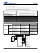
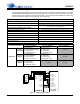
Table Of Contents
- 1. Characteristics and Specifications
- Specified Operating Conditions
- Absolute Maximum Ratings
- Analog Input Characteristics
- A/D Digital Filter Characteristics
- Analog Output Characteristics
- D/A Digital Filter Characteristics
- Switching Characteristics
- Switching Characteristics - Control Port - I²C™ Format
- Switching Characteristics - Control Port - SPI™ Format
- DC Electrical Characteristics
- Digital Interface Characteristics
- 2. Pin Descriptions
- 3. Typical Connection Diagram
- 4. Applications
- 4.1 Overview
- 4.2 Analog Inputs
- 4.3 Analog Outputs
- 4.4 S/PDIF Receiver
- 4.5 Clock Generation
- 4.6 Digital Interfaces
- 4.7 Control Port Description and Timing
- 4.8 Interrupts
- 4.9 Reset and Power-Up
- 4.10 Power Supply, Grounding, and PCB Layout
- 5. Register Quick Reference
- 6. Register Description
- Table 5. DAC De-Emphasis
- Table 6. Receiver De-Emphasis
- Table 7. Digital Interface Formats
- Table 8. ADC One-Line Mode
- Table 9. DAC One-Line Mode
- Table 10. RMCK Divider Settings
- Table 11. OMCK Frequency Settings
- Table 12. Master Clock Source Select
- Table 13. AES Format Detection
- Table 14. Receiver Clock Frequency Detection
- Table 15. Example Digital Volume Settings
- Table 16. ATAPI Decode
- Table 17. Example ADC Input Gain Settings
- Table 18. TXP Output Selection
- Table 19. Receiver Input Selection
- Table 20. Auxiliary Data Width Selection
- 7. Parameter Definitions
- 8. Appendix A: External Filters
- 9. Appendix B: S/PDIF Receiver
- 10. Appendix C: PLL Filter
- 11. Appendix D: External AES3-S/PDIF-IEC60958 Receiver Components
- 12. Appendix E: ADC Filter Plots
- Figure 34. Single-Speed Mode Stopband Rejection
- Figure 35. Single-Speed Mode Transition Band
- Figure 36. Single-Speed Mode Transition Band (Detail)
- Figure 37. Single-Speed Mode Passband Ripple
- Figure 38. Double-Speed Mode Stopband Rejection
- Figure 39. Double-Speed Mode Transition Band
- Figure 40. Double-Speed Mode Transition Band (Detail)
- Figure 41. Double-Speed Mode Passband Ripple
- Figure 42. Quad-Speed Mode Stopband Rejection
- Figure 43. Quad-Speed Mode Transition Band
- Figure 44. Quad-Speed Mode Transition Band (Detail)
- Figure 45. Quad-Speed Mode Passband Ripple
- 13. Appendix F: DAC Filter Plots
- Figure 46. Single-Speed (fast) Stopband Rejection
- Figure 47. Single-Speed (fast) Transition Band
- Figure 48. Single-Speed (fast) Transition Band (detail)
- Figure 49. Single-Speed (fast) Passband Ripple
- Figure 50. Single-Speed (slow) Stopband Rejection
- Figure 51. Single-Speed (slow) Transition Band
- Figure 52. Single-Speed (slow) Transition Band (detail)
- Figure 53. Single-Speed (slow) Passband Ripple
- Figure 54. Double-Speed (fast) Stopband Rejection
- Figure 55. Double-Speed (fast) Transition Band
- Figure 56. Double-Speed (fast) Transition Band (detail)
- Figure 57. Double-Speed (fast) Passband Ripple
- Figure 58. Double-Speed (slow) Stopband Rejection
- Figure 59. Double-Speed (slow) Transition Band
- Figure 60. Double-Speed (slow) Transition Band (detail)
- Figure 61. Double-Speed (slow) Passband Ripple
- Figure 62. Quad-Speed (fast) Stopband Rejection
- Figure 63. Quad-Speed (fast) Transition Band
- Figure 64. Quad-Speed (fast) Transition Band (detail)
- Figure 65. Quad-Speed (fast) Passband Ripple
- Figure 66. Quad-Speed (slow) Stopband Rejection
- Figure 67. Quad-Speed (slow) Transition Band
- Figure 68. Quad-Speed (slow) Transition Band (detail)
- Figure 69. Quad-Speed (slow) Passband Ripple
- 14. Package Dimensions
- 15. Ordering Information
- 16. References
- 17. Revision History
38 DS583F2
CS42516
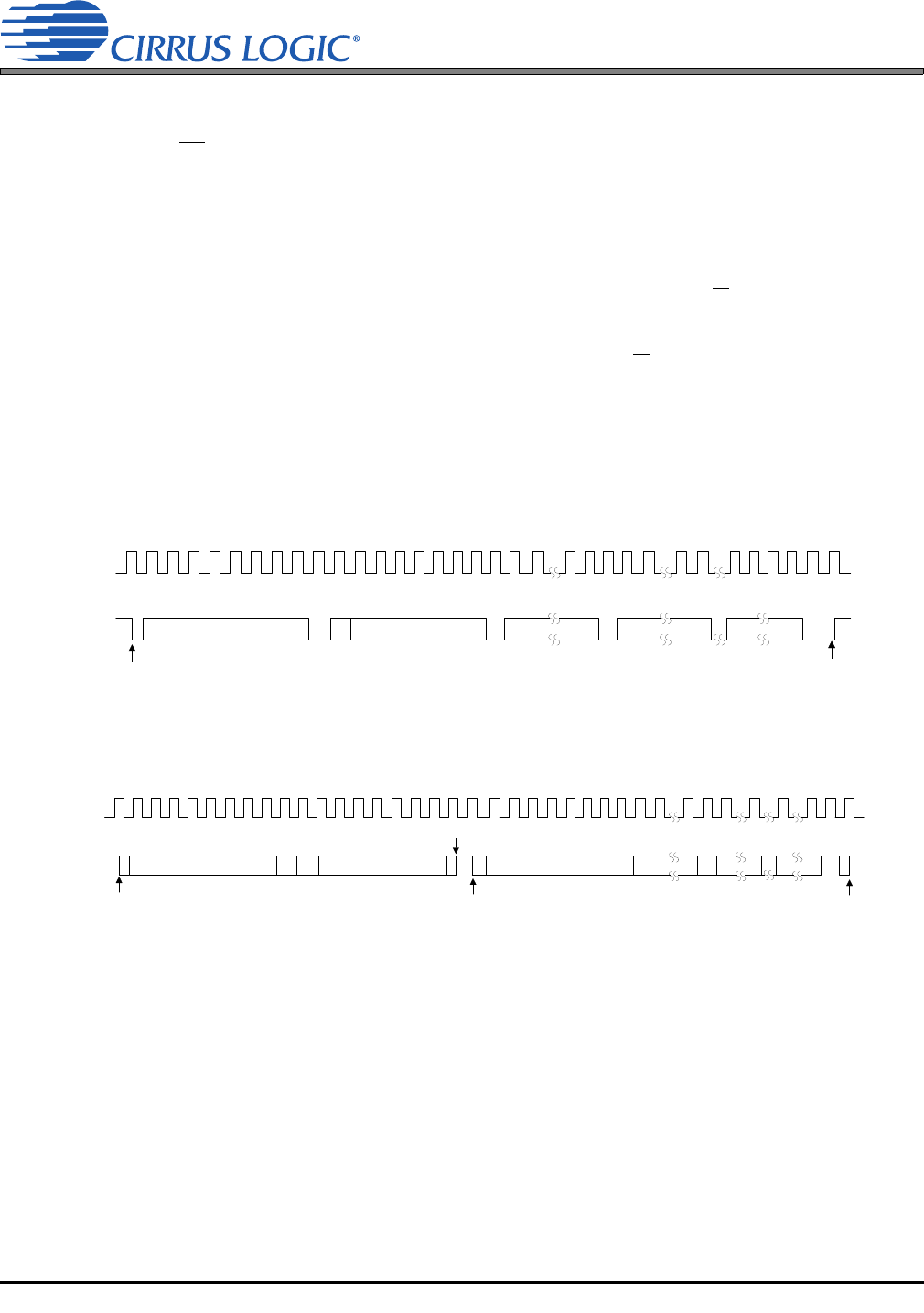
4.7.2 I²C Mode
In I²C mode, SDA is a bidirectional data line. Data is clocked into and out of the part by the clock, SCL.
There is no CS
pin. Pins AD0 and AD1 form the two least-significant bits of the chip address and should
be connected through a resistor to VLC or DGND as desired. The state of the pins is sensed while the
CS42516 is being reset.
The signal timings for a read and write cycle are shown in Figure 22 and Figure 23. A Start condition is
defined as a falling transition of SDA while the clock is high. A Stop condition is a rising transition while
the clock is high. All other transitions of SDA occur while the clock is low. The first byte sent to the
CS42516 after a Start condition consists of a 7-bit chip address field and a R/W
bit (high for a read, low
for a write). The upper 5 bits of the 7-bit address field are fixed at 10011. To communicate with a CS42516,
the chip address field, which is the first byte sent to the CS42516, should match 10011, followed by the
settings of the AD1 and AD0. The eighth bit of the address is the R/W
bit. If the operation is a write, the
next byte is the Memory Address Pointer (MAP) which selects the register to be read or written. If the op-
eration is a read, the contents of the register pointed to by the MAP will be output. Setting the auto-incre-
ment bit in MAP allows successive reads or writes of consecutive registers. Each byte is separated by an
acknowledge bit. The ACK bit is output from the CS42516 after each input byte is read and is input to the
CS42516 from the microcontroller after each transmitted byte.
Since the read operation cannot set the MAP, an aborted write operation is used as a preamble. As shown
in Figure 23, the write operation is aborted after the acknowledge for the MAP byte by sending a stop con-
dition. The following pseudocode illustrates an aborted write operation followed by a read operation.
Send start condition.
Send 10011xx0 (chip address & write operation).
Receive acknowledge bit.
Send MAP byte, auto increment off.
Receive acknowledge bit.
Send stop condition, aborting write.
4 5 6 7 24 25
SCL
CHIP ADDRESS (WRITE) MAP BYTE DATA
DATA +1
START
ACK
STOP
ACKACKACK
1 0 0 1 1 AD1 AD0 0
SDA
INCR 6 5 4 3 2 1 0 7 6 1 0 7 6 1 0 7 6 1 0
0 1 2 3 8 9 12 16 17 18 1910 11 13 14 15 27 28
26
DATA +n
Figure 22. Control Port Timing, I²C Write
SCL
CHIP ADDRESS (WRITE)
MAP BYTE
DATA
DATA +1
START
ACK
STOP
ACK
ACK
ACK
1 0 0 1 1 AD1 AD0 0
SDA
1 0 0 1 1 AD1 AD0 1
CHIP ADDRESS (READ)
START
INCR 6 5 4 3 2 1 0
7 0 7 0 7 0
NO
168 9 12 13 14 154 5 6 7 0 1 20 21 22 23 24
26 27 28
2 3 10 11 17 18 19 25
ACK
DATA + n
STOP
Figure 23. Control Port Timing, I²C Read