
User guide
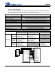
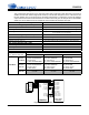
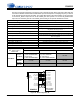
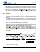
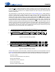
Table Of Contents
- 1. Characteristics and Specifications
- Specified Operating Conditions
- Absolute Maximum Ratings
- Analog Input Characteristics
- A/D Digital Filter Characteristics
- Analog Output Characteristics
- D/A Digital Filter Characteristics
- Switching Characteristics
- Switching Characteristics - Control Port - I²C™ Format
- Switching Characteristics - Control Port - SPI™ Format
- DC Electrical Characteristics
- Digital Interface Characteristics
- 2. Pin Descriptions
- 3. Typical Connection Diagram
- 4. Applications
- 4.1 Overview
- 4.2 Analog Inputs
- 4.3 Analog Outputs
- 4.4 S/PDIF Receiver
- 4.5 Clock Generation
- 4.6 Digital Interfaces
- 4.7 Control Port Description and Timing
- 4.8 Interrupts
- 4.9 Reset and Power-Up
- 4.10 Power Supply, Grounding, and PCB Layout
- 5. Register Quick Reference
- 6. Register Description
- Table 5. DAC De-Emphasis
- Table 6. Receiver De-Emphasis
- Table 7. Digital Interface Formats
- Table 8. ADC One-Line Mode
- Table 9. DAC One-Line Mode
- Table 10. RMCK Divider Settings
- Table 11. OMCK Frequency Settings
- Table 12. Master Clock Source Select
- Table 13. AES Format Detection
- Table 14. Receiver Clock Frequency Detection
- Table 15. Example Digital Volume Settings
- Table 16. ATAPI Decode
- Table 17. Example ADC Input Gain Settings
- Table 18. TXP Output Selection
- Table 19. Receiver Input Selection
- Table 20. Auxiliary Data Width Selection
- 7. Parameter Definitions
- 8. Appendix A: External Filters
- 9. Appendix B: S/PDIF Receiver
- 10. Appendix C: PLL Filter
- 11. Appendix D: External AES3-S/PDIF-IEC60958 Receiver Components
- 12. Appendix E: ADC Filter Plots
- Figure 34. Single-Speed Mode Stopband Rejection
- Figure 35. Single-Speed Mode Transition Band
- Figure 36. Single-Speed Mode Transition Band (Detail)
- Figure 37. Single-Speed Mode Passband Ripple
- Figure 38. Double-Speed Mode Stopband Rejection
- Figure 39. Double-Speed Mode Transition Band
- Figure 40. Double-Speed Mode Transition Band (Detail)
- Figure 41. Double-Speed Mode Passband Ripple
- Figure 42. Quad-Speed Mode Stopband Rejection
- Figure 43. Quad-Speed Mode Transition Band
- Figure 44. Quad-Speed Mode Transition Band (Detail)
- Figure 45. Quad-Speed Mode Passband Ripple
- 13. Appendix F: DAC Filter Plots
- Figure 46. Single-Speed (fast) Stopband Rejection
- Figure 47. Single-Speed (fast) Transition Band
- Figure 48. Single-Speed (fast) Transition Band (detail)
- Figure 49. Single-Speed (fast) Passband Ripple
- Figure 50. Single-Speed (slow) Stopband Rejection
- Figure 51. Single-Speed (slow) Transition Band
- Figure 52. Single-Speed (slow) Transition Band (detail)
- Figure 53. Single-Speed (slow) Passband Ripple
- Figure 54. Double-Speed (fast) Stopband Rejection
- Figure 55. Double-Speed (fast) Transition Band
- Figure 56. Double-Speed (fast) Transition Band (detail)
- Figure 57. Double-Speed (fast) Passband Ripple
- Figure 58. Double-Speed (slow) Stopband Rejection
- Figure 59. Double-Speed (slow) Transition Band
- Figure 60. Double-Speed (slow) Transition Band (detail)
- Figure 61. Double-Speed (slow) Passband Ripple
- Figure 62. Quad-Speed (fast) Stopband Rejection
- Figure 63. Quad-Speed (fast) Transition Band
- Figure 64. Quad-Speed (fast) Transition Band (detail)
- Figure 65. Quad-Speed (fast) Passband Ripple
- Figure 66. Quad-Speed (slow) Stopband Rejection
- Figure 67. Quad-Speed (slow) Transition Band
- Figure 68. Quad-Speed (slow) Transition Band (detail)
- Figure 69. Quad-Speed (slow) Passband Ripple
- 14. Package Dimensions
- 15. Ordering Information
- 16. References
- 17. Revision History
34 DS583F2
CS42516
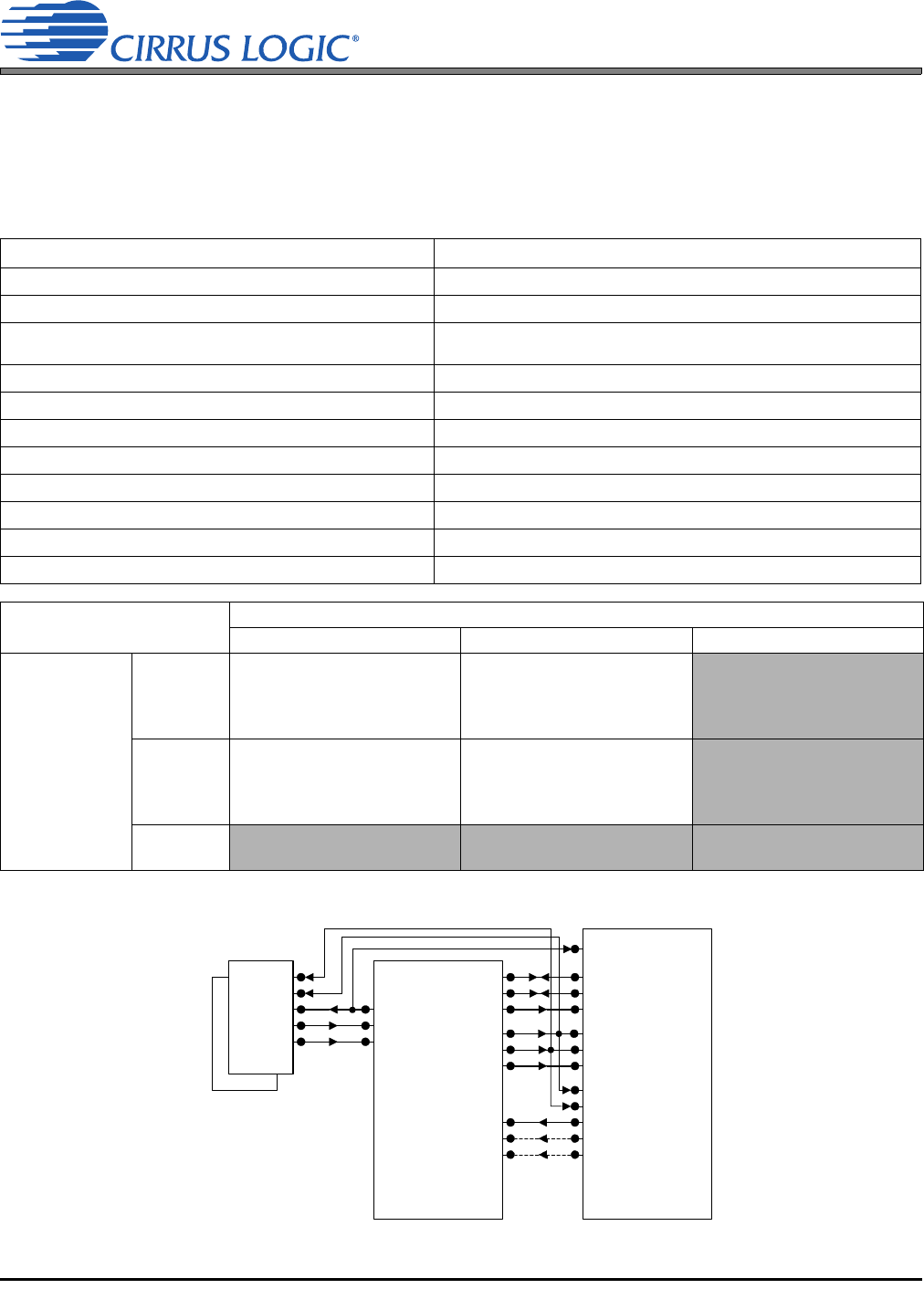
4.6.4.3 OLM Config #3
This One Line Mode configuration #3 will support up to 6 channels of DAC data, 6 channels of ADC data and 2
channels of S/PDIF received data and will handle up to 20-bit samples at a sampling frequency of 48kHz on all
channels for both the DAC and ADC. The output data stream of the internal and external ADCs is configured to use
the CX_SDOUT output and run at the CODEC_SP clock speeds. One Line Mode #2, which supports 24-bit sam-
ples, is not supported by this configuration.
Register / Bit Settings Description
Functional Mode Register (addr = 03h)
Set CODEC_FMx = SAI_FMx = 00,01,10
CX_LRCK must equal SAI_LRCK; sample rate conversion not supported
Set ADC_SP SELx = 00
Configure ADC data to use CX_SDOUT and CODEC_SP Clocks. S/PDIF
data is supported on SAI_SDOUT
Interface Format Register (addr = 04h)
Set DIFx bits to proper serial format
Select the digital interface format when not in one line mode
Set ADC_OLx bits = 00,01
Select ADC operating mode, see table below for valid combinations
Set DAC_OLx bits = 00,01
Select DAC operating mode, see table below for valid combinations
Misc. Control Register (addr = 05h)
Set CODEC_SP M/S = 1
Set CODEC Serial Port to master mode.
Set SAI_SP M/S = 0 or 1
Set Serial Audio Interface Port to master mode or slave mode.
Set EXT ADC SCLK = 1
Identify external ADC clock source as CODEC Serial Port.
CX_SDOUT= ADC Data
SAI_SDOUT=S/PDIF Data
DAC Mode
Not One Line Mode One Line Mode #1 One Line Mode #2
ADC Mode
Not One-
Line Mode
CX_SCLK=64 Fs
CX_LRCK=SSM/DSM/QSM
SAI_SCLK=64 Fs
SAI_LRCK=CX_LRCK
CX_SCLK=128 Fs
CX_LRCK=SSM
SAI_SCLK=64 Fs
SAI_LRCK=CX_LRCK
not valid
One-Line
Mode #1
CX_SCLK=128 Fs
CX_LRCK=SSM
SAI_SCLK=64 Fs
SAI_LRCK=CX_LRCK
CX_SCLK=128 Fs
CX_LRCK=SSM
SAI_SCLK=64 Fs
SAI_LRCK=CX_LRCK
not valid
One-Line
Mode #2
not valid not valid not valid
Figure 18. OLM Configuration #3
SCLK_PORT1
LRCK_PORT1
SDIN_PORT1
SCLK_PORT2
LRCK_PORT2
SDIN_PORT2
SCLK_PORT3
LRCK_PORT3
SDOUT1_PORT3
SDOUT2_PORT3
SDOUT3_PORT3
RMCK
ADCIN1
ADCIN2
MCLK
SDOUT1
SDOUT2
LRCK
SCLK
64Fs
SPDIF Data
ADC Data
64Fs,128Fs
DIGITAL AUDIO
PROCESSOR
CS5361
CS5361
SAI_SCLK
SAI_LRCK
SAI_SDOUT
CX_SCLK
CX_LRCK
CX_SDOUT
CX_SDIN1
CX_SDIN2
CX_SDIN3
MCLK
CS42516