
User guide
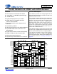
Table Of Contents
- 1. Characteristics and Specifications
- Specified Operating Conditions
- Absolute Maximum Ratings
- Analog Input Characteristics
- A/D Digital Filter Characteristics
- Analog Output Characteristics
- D/A Digital Filter Characteristics
- Switching Characteristics
- Switching Characteristics - Control Port - I²C™ Format
- Switching Characteristics - Control Port - SPI™ Format
- DC Electrical Characteristics
- Digital Interface Characteristics
- 2. Pin Descriptions
- 3. Typical Connection Diagram
- 4. Applications
- 4.1 Overview
- 4.2 Analog Inputs
- 4.3 Analog Outputs
- 4.4 S/PDIF Receiver
- 4.5 Clock Generation
- 4.6 Digital Interfaces
- 4.7 Control Port Description and Timing
- 4.8 Interrupts
- 4.9 Reset and Power-Up
- 4.10 Power Supply, Grounding, and PCB Layout
- 5. Register Quick Reference
- 6. Register Description
- Table 5. DAC De-Emphasis
- Table 6. Receiver De-Emphasis
- Table 7. Digital Interface Formats
- Table 8. ADC One-Line Mode
- Table 9. DAC One-Line Mode
- Table 10. RMCK Divider Settings
- Table 11. OMCK Frequency Settings
- Table 12. Master Clock Source Select
- Table 13. AES Format Detection
- Table 14. Receiver Clock Frequency Detection
- Table 15. Example Digital Volume Settings
- Table 16. ATAPI Decode
- Table 17. Example ADC Input Gain Settings
- Table 18. TXP Output Selection
- Table 19. Receiver Input Selection
- Table 20. Auxiliary Data Width Selection
- 7. Parameter Definitions
- 8. Appendix A: External Filters
- 9. Appendix B: S/PDIF Receiver
- 10. Appendix C: PLL Filter
- 11. Appendix D: External AES3-S/PDIF-IEC60958 Receiver Components
- 12. Appendix E: ADC Filter Plots
- Figure 34. Single-Speed Mode Stopband Rejection
- Figure 35. Single-Speed Mode Transition Band
- Figure 36. Single-Speed Mode Transition Band (Detail)
- Figure 37. Single-Speed Mode Passband Ripple
- Figure 38. Double-Speed Mode Stopband Rejection
- Figure 39. Double-Speed Mode Transition Band
- Figure 40. Double-Speed Mode Transition Band (Detail)
- Figure 41. Double-Speed Mode Passband Ripple
- Figure 42. Quad-Speed Mode Stopband Rejection
- Figure 43. Quad-Speed Mode Transition Band
- Figure 44. Quad-Speed Mode Transition Band (Detail)
- Figure 45. Quad-Speed Mode Passband Ripple
- 13. Appendix F: DAC Filter Plots
- Figure 46. Single-Speed (fast) Stopband Rejection
- Figure 47. Single-Speed (fast) Transition Band
- Figure 48. Single-Speed (fast) Transition Band (detail)
- Figure 49. Single-Speed (fast) Passband Ripple
- Figure 50. Single-Speed (slow) Stopband Rejection
- Figure 51. Single-Speed (slow) Transition Band
- Figure 52. Single-Speed (slow) Transition Band (detail)
- Figure 53. Single-Speed (slow) Passband Ripple
- Figure 54. Double-Speed (fast) Stopband Rejection
- Figure 55. Double-Speed (fast) Transition Band
- Figure 56. Double-Speed (fast) Transition Band (detail)
- Figure 57. Double-Speed (fast) Passband Ripple
- Figure 58. Double-Speed (slow) Stopband Rejection
- Figure 59. Double-Speed (slow) Transition Band
- Figure 60. Double-Speed (slow) Transition Band (detail)
- Figure 61. Double-Speed (slow) Passband Ripple
- Figure 62. Quad-Speed (fast) Stopband Rejection
- Figure 63. Quad-Speed (fast) Transition Band
- Figure 64. Quad-Speed (fast) Transition Band (detail)
- Figure 65. Quad-Speed (fast) Passband Ripple
- Figure 66. Quad-Speed (slow) Stopband Rejection
- Figure 67. Quad-Speed (slow) Transition Band
- Figure 68. Quad-Speed (slow) Transition Band (detail)
- Figure 69. Quad-Speed (slow) Passband Ripple
- 14. Package Dimensions
- 15. Ordering Information
- 16. References
- 17. Revision History

DS583F2 3
CS42516
6. REGISTER DESCRIPTION .................................................................................................................. 45
6.1 Memory Address Pointer (MAP) ..................................................................................................... 45
6.2 Chip I.D. and Revision Register (address 01h) (Read Only) .......................................................... 45
6.3 Power Control (address 02h) .......................................................................................................... 46
6.4 Functional Mode (address 03h) ...................................................................................................... 47
6.5 Interface Formats (address 04h) .................................................................................................... 49
6.6 Misc Control (address 05h) ............................................................................................................ 50
6.7 Clock Control (address 06h) ........................................................................................................... 52
6.8 OMCK/PLL_CLK Ratio (address 07h) (Read Only) ....................................................................... 53
6.9 RVCR Status (address 08h) (Read Only) ....................................................................................... 54
6.10 Burst Preamble PC and PD Bytes (addresses 09h - 0Ch)(Read Only) ........................................ 55
6.11 Volume Transition Control (address 0Dh) .................................................................................... 56
6.12 Channel Mute (address 0Eh) ........................................................................................................ 58
6.13 Volume Control (addresses 0Fh, 10h, 11h, 12h, 13h, 14h) ...................................................... 58
6.14 Channel Invert (address 17h) ....................................................................................................... 58
6.15 Mixing Control Pair 1 (Channels A1 & B1) (address 18h)
Mixing Control Pair 2 (Channels A2 & B2) (address 19h)
Mixing Control Pair 3 (Channels A3 & B3) (address 1Ah) ............................................................ 58
6.16 ADC Left Channel Gain (address 1Ch) ........................................................................................ 61
6.17 ADC Right Channel Gain (address 1Dh) ......................................................................................61
6.18 Receiver Mode Control (address 1Eh) ......................................................................................... 61
6.19 Receiver Mode Control 2 (address 1Fh) ...................................................................................... 63
6.20 Interrupt Status (address 20h) (Read Only) ................................................................................. 63
6.21 Interrupt Mask (address 21h) ....................................................................................................... 64
6.22 Interrupt Mode MSB (address 22h)
Interrupt Mode LSB (address 23h) ...............................................................................................65
6.23 Channel Status Data Buffer Control (address 24h) ...................................................................... 65
6.24 Receiver Channel Status (address 25h) (Read Only) .................................................................. 66
6.25 Receiver Errors (address 26h) (Read Only) .................................................................................67
6.26 Receiver Errors Mask (address 27h) ............................................................................................ 68
6.27 Mutec Pin Control (address 28h) .................................................................................................. 69
6.28 RXP/General-Purpose Pin Control (addresses 29h to 2Fh) ......................................................... 69
6.29 Q-Channel Subcode Bytes 0 to 9 (addresses 30h to 39h) (Read Only) ....................................... 71
6.30 C-Bit or U-Bit Data Buffer (addresses 3Ah to 51h) (Read Only) .................................................. 71
7. PARAMETER DEFINITIONS ................................................................................................................ 72
8. APPENDIX A: EXTERNAL FILTERS ................................................................................................... 73
8.1 ADC Input Filter .............................................................................................................................. 73
8.2 DAC Output Filter ........................................................................................................................... 73
9. APPENDIX B: S/PDIF RECEIVER ....................................................................................................... 74
9.1 Error Reporting and Hold Function ................................................................................................. 74
9.2 Channel Status Data Handling ....................................................................................................... 74
9.2.1 Channel Status Data E Buffer Access ................................................................................... 75
9.2.1.1 One-Byte Mode ..........................................................................................................75
9.2.1.2 Two-Byte Mode ..........................................................................................................75
9.2.2 Serial Copy Management System (SCMS) ........................................................................... 76
9.3 User (U) Data E Buffer Access ....................................................................................................... 76
9.3.1 Non-Audio Auto-Detection ..................................................................................................... 76
9.3.1.1 Format Detection .......................................................................................................76
10. APPENDIX C: PLL FILTER ....................................................................................................
............ 77
10.1 External Filter Components .......................................................................................................... 77
10.1.1 General ................................................................................................................................ 77
10.1.2 Jitter Attenuation ................................................................................................................. 79
10.1.3 Capacitor Selection ............................................................................................................. 80
10.1.4 Circuit Board Layout ............................................................................................................ 81