
User guide
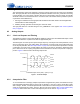
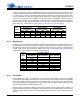
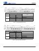
Table Of Contents
- 1. Characteristics and Specifications
- Specified Operating Conditions
- Absolute Maximum Ratings
- Analog Input Characteristics
- A/D Digital Filter Characteristics
- Analog Output Characteristics
- D/A Digital Filter Characteristics
- Switching Characteristics
- Switching Characteristics - Control Port - I²C™ Format
- Switching Characteristics - Control Port - SPI™ Format
- DC Electrical Characteristics
- Digital Interface Characteristics
- 2. Pin Descriptions
- 3. Typical Connection Diagram
- 4. Applications
- 4.1 Overview
- 4.2 Analog Inputs
- 4.3 Analog Outputs
- 4.4 S/PDIF Receiver
- 4.5 Clock Generation
- 4.6 Digital Interfaces
- 4.7 Control Port Description and Timing
- 4.8 Interrupts
- 4.9 Reset and Power-Up
- 4.10 Power Supply, Grounding, and PCB Layout
- 5. Register Quick Reference
- 6. Register Description
- Table 5. DAC De-Emphasis
- Table 6. Receiver De-Emphasis
- Table 7. Digital Interface Formats
- Table 8. ADC One-Line Mode
- Table 9. DAC One-Line Mode
- Table 10. RMCK Divider Settings
- Table 11. OMCK Frequency Settings
- Table 12. Master Clock Source Select
- Table 13. AES Format Detection
- Table 14. Receiver Clock Frequency Detection
- Table 15. Example Digital Volume Settings
- Table 16. ATAPI Decode
- Table 17. Example ADC Input Gain Settings
- Table 18. TXP Output Selection
- Table 19. Receiver Input Selection
- Table 20. Auxiliary Data Width Selection
- 7. Parameter Definitions
- 8. Appendix A: External Filters
- 9. Appendix B: S/PDIF Receiver
- 10. Appendix C: PLL Filter
- 11. Appendix D: External AES3-S/PDIF-IEC60958 Receiver Components
- 12. Appendix E: ADC Filter Plots
- Figure 34. Single-Speed Mode Stopband Rejection
- Figure 35. Single-Speed Mode Transition Band
- Figure 36. Single-Speed Mode Transition Band (Detail)
- Figure 37. Single-Speed Mode Passband Ripple
- Figure 38. Double-Speed Mode Stopband Rejection
- Figure 39. Double-Speed Mode Transition Band
- Figure 40. Double-Speed Mode Transition Band (Detail)
- Figure 41. Double-Speed Mode Passband Ripple
- Figure 42. Quad-Speed Mode Stopband Rejection
- Figure 43. Quad-Speed Mode Transition Band
- Figure 44. Quad-Speed Mode Transition Band (Detail)
- Figure 45. Quad-Speed Mode Passband Ripple
- 13. Appendix F: DAC Filter Plots
- Figure 46. Single-Speed (fast) Stopband Rejection
- Figure 47. Single-Speed (fast) Transition Band
- Figure 48. Single-Speed (fast) Transition Band (detail)
- Figure 49. Single-Speed (fast) Passband Ripple
- Figure 50. Single-Speed (slow) Stopband Rejection
- Figure 51. Single-Speed (slow) Transition Band
- Figure 52. Single-Speed (slow) Transition Band (detail)
- Figure 53. Single-Speed (slow) Passband Ripple
- Figure 54. Double-Speed (fast) Stopband Rejection
- Figure 55. Double-Speed (fast) Transition Band
- Figure 56. Double-Speed (fast) Transition Band (detail)
- Figure 57. Double-Speed (fast) Passband Ripple
- Figure 58. Double-Speed (slow) Stopband Rejection
- Figure 59. Double-Speed (slow) Transition Band
- Figure 60. Double-Speed (slow) Transition Band (detail)
- Figure 61. Double-Speed (slow) Passband Ripple
- Figure 62. Quad-Speed (fast) Stopband Rejection
- Figure 63. Quad-Speed (fast) Transition Band
- Figure 64. Quad-Speed (fast) Transition Band (detail)
- Figure 65. Quad-Speed (fast) Passband Ripple
- Figure 66. Quad-Speed (slow) Stopband Rejection
- Figure 67. Quad-Speed (slow) Transition Band
- Figure 68. Quad-Speed (slow) Transition Band (detail)
- Figure 69. Quad-Speed (slow) Passband Ripple
- 14. Package Dimensions
- 15. Ordering Information
- 16. References
- 17. Revision History
26 DS583F2
CS42516
When either serial port is in Slave Mode, its respective LRCK signal must be present for proper device
operation.
In Slave Mode, One-Line Mode #1 is supported; One-Line Mode #2 is not.
The sample rate to OMCK ratios and OMCK frequency requirements for Slave Mode operation are shown
in Table 1. Refer to Table 3 for required clock ratios.
4.6 Digital Interfaces
4.6.1 Serial Audio Interface Signals
The CS42516 interfaces to an external Digital Audio Processor via two independent serial ports, the
CODEC serial port, CODEC_SP and the Serial Audio Interface serial port, SAI_SP. The digital output of
the internal ADCs can be configured to use either the CX_SDOUT pin or the SAI_SDOUT pin and the
corresponding serial port clocking signals. These configuration bits and the selection of Single-, Double-
or Quad-Speed Mode for CODEC_SP and SAI_SP are found in register “Functional Mode (address 03h)”
on page 47.
The serial interface clocks, SAI_SCLK for SAI_SP and CX_SCLK for CODEC_SP, are used for transmit-
ting and receiving audio data. Either SAI_SCLK or CX_SCLK can be generated by the CS42516 (Master
Mode), or it can be input from an external source (Slave Mode). Master or Slave Mode selection is made
using bits CODEC_SP M/S
and SAI_SP M/S in register “Misc Control (address 05h)” on page 50.
The Left/Right clock (SAI_LRCK or CX_LRCK) is used to indicate left and right data frames and the start
of a new sample period. It may be an output of the CS42516 (Master Mode), or it may be generated by
an external source (Slave Mode). As described in later sections, particular modes of operation do allow
the sample rate, Fs, of the SAI_SP and the CODEC_SP to be different, but must be multiples of each
other.
The serial data interface format selection (Left/Right-Justified, I²S or One-Line Mode) for the Serial Audio
Interface serial port data out pin, SAI_SDOUT, the CODEC serial port data out pin, CX_SDOUT, and the
CODEC input pins, CX_SDIN1:3, is configured using the appropriate bits in the register “Interface For-
mats (address 04h)” on page 49. The serial audio data is presented in two's complement binary form with
the MSB first in all formats.
CX_SDIN1, CX_SDIN2, and CX_SDIN3 are the serial data input pins supplying the associated internal
DAC. CX_SDOUT, the ADC data output pin, carries data from the two internal 24-bit ADCs and, when
configured for one-line mode, up to four additional ADC channels attached externally to the signals AD-
CIN1 and ADCIN2 (typically two CS5361 stereo ADCs). When operated in One-Line Mode, 6 channels of
DAC data are input on CX_SDIN1 and 6 channels of ADC data are output on CX_SDOUT. Table 4 on
page 27 outlines the serial port channel allocations.
Single-Speed Double-Speed Quad-Speed One-Line Mode #1
OMCK/LRCK Ratio
256x, 384x, 512x 128x, 192x, 256x 64x, 96x, 128x 256x
SCLK/LRCK Ratio
32x, 48x, 64x, 128x 32x, 48x, 64x 32x, 48x, 64x 128x
Table 3. Slave Mode Clock Ratios