
User guide
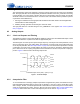
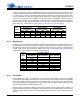
Table Of Contents
- 1. Characteristics and Specifications
- Specified Operating Conditions
- Absolute Maximum Ratings
- Analog Input Characteristics
- A/D Digital Filter Characteristics
- Analog Output Characteristics
- D/A Digital Filter Characteristics
- Switching Characteristics
- Switching Characteristics - Control Port - I²C™ Format
- Switching Characteristics - Control Port - SPI™ Format
- DC Electrical Characteristics
- Digital Interface Characteristics
- 2. Pin Descriptions
- 3. Typical Connection Diagram
- 4. Applications
- 4.1 Overview
- 4.2 Analog Inputs
- 4.3 Analog Outputs
- 4.4 S/PDIF Receiver
- 4.5 Clock Generation
- 4.6 Digital Interfaces
- 4.7 Control Port Description and Timing
- 4.8 Interrupts
- 4.9 Reset and Power-Up
- 4.10 Power Supply, Grounding, and PCB Layout
- 5. Register Quick Reference
- 6. Register Description
- Table 5. DAC De-Emphasis
- Table 6. Receiver De-Emphasis
- Table 7. Digital Interface Formats
- Table 8. ADC One-Line Mode
- Table 9. DAC One-Line Mode
- Table 10. RMCK Divider Settings
- Table 11. OMCK Frequency Settings
- Table 12. Master Clock Source Select
- Table 13. AES Format Detection
- Table 14. Receiver Clock Frequency Detection
- Table 15. Example Digital Volume Settings
- Table 16. ATAPI Decode
- Table 17. Example ADC Input Gain Settings
- Table 18. TXP Output Selection
- Table 19. Receiver Input Selection
- Table 20. Auxiliary Data Width Selection
- 7. Parameter Definitions
- 8. Appendix A: External Filters
- 9. Appendix B: S/PDIF Receiver
- 10. Appendix C: PLL Filter
- 11. Appendix D: External AES3-S/PDIF-IEC60958 Receiver Components
- 12. Appendix E: ADC Filter Plots
- Figure 34. Single-Speed Mode Stopband Rejection
- Figure 35. Single-Speed Mode Transition Band
- Figure 36. Single-Speed Mode Transition Band (Detail)
- Figure 37. Single-Speed Mode Passband Ripple
- Figure 38. Double-Speed Mode Stopband Rejection
- Figure 39. Double-Speed Mode Transition Band
- Figure 40. Double-Speed Mode Transition Band (Detail)
- Figure 41. Double-Speed Mode Passband Ripple
- Figure 42. Quad-Speed Mode Stopband Rejection
- Figure 43. Quad-Speed Mode Transition Band
- Figure 44. Quad-Speed Mode Transition Band (Detail)
- Figure 45. Quad-Speed Mode Passband Ripple
- 13. Appendix F: DAC Filter Plots
- Figure 46. Single-Speed (fast) Stopband Rejection
- Figure 47. Single-Speed (fast) Transition Band
- Figure 48. Single-Speed (fast) Transition Band (detail)
- Figure 49. Single-Speed (fast) Passband Ripple
- Figure 50. Single-Speed (slow) Stopband Rejection
- Figure 51. Single-Speed (slow) Transition Band
- Figure 52. Single-Speed (slow) Transition Band (detail)
- Figure 53. Single-Speed (slow) Passband Ripple
- Figure 54. Double-Speed (fast) Stopband Rejection
- Figure 55. Double-Speed (fast) Transition Band
- Figure 56. Double-Speed (fast) Transition Band (detail)
- Figure 57. Double-Speed (fast) Passband Ripple
- Figure 58. Double-Speed (slow) Stopband Rejection
- Figure 59. Double-Speed (slow) Transition Band
- Figure 60. Double-Speed (slow) Transition Band (detail)
- Figure 61. Double-Speed (slow) Passband Ripple
- Figure 62. Quad-Speed (fast) Stopband Rejection
- Figure 63. Quad-Speed (fast) Transition Band
- Figure 64. Quad-Speed (fast) Transition Band (detail)
- Figure 65. Quad-Speed (fast) Passband Ripple
- Figure 66. Quad-Speed (slow) Stopband Rejection
- Figure 67. Quad-Speed (slow) Transition Band
- Figure 68. Quad-Speed (slow) Transition Band (detail)
- Figure 69. Quad-Speed (slow) Passband Ripple
- 14. Package Dimensions
- 15. Ordering Information
- 16. References
- 17. Revision History
24 DS583F2
CS42516
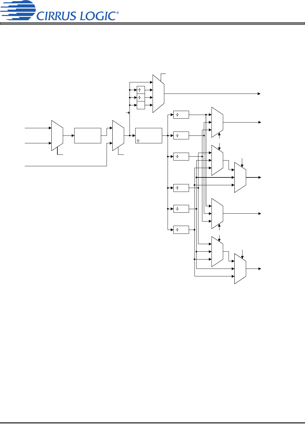
4.5 Clock Generation
The clock generation for the CS42516 is shown in the figure below. The internal MCLK is derived from the
output of the PLL or a master clock source attached to OMCK. The mux selection is controlled by the SW_C-
TRLx bits and can be configured to manual switch mode only, or automatically switch on loss of PLL lock
to the other source input.
4.5.1 PLL and Jitter Attenuation
An on-chip Phase Locked Loop (PLL) is used to recover the clock from the incoming S/PDIF data stream.
There are some applications where low jitter in the recovered clock, presented on the RMCK pin, is im-
portant. For this reason, the PLL has been designed to have good jitter attenuation characteristics as
shown in Figure 28 on page 79.
The PLL can be configured to lock onto the incoming SAI_LRCK signal from the Serial Audio Interface
Port and generate the required internal master clock frequency. By setting the PLL_LRCK bit to a ‘1’ in
the register “Clock Control (address 06h)” on page 52, the PLL will lock to the incoming SAI_LRCK and
generate an output master clock (RMCK) of 256Fs. Table 2 shows the output of the PLL with typical input
Fs values for SAI_LRCK.
See “Appendix C: PLL Filter” on page 77 for more information concerning PLL operation, required filter
components, optimal layout guidelines, and jitter-attenuation characteristics.
SAI_LRCK
(slave mode)
Recovered
S/PDIF Clock
0
1
PLL (256Fs)
8.192 -
49.152 MHz
00
01
PLL_LRCK bit
SW_CTRLx bits
(manual or auto
switch)
OMCK
Auto Detect
Input Clock
1,1.5, 2, 4
single
speed
256
double
speed
128
quad
speed
64
single
speed
4
double
speed
2
quad
speed
1
00
01
10
00
01
10
00
01
10
00
01
10
not OLM
OLM #1
CODEC_FMx bits
SAI_FMx bits
DAC_OLx
or ADC_OLx bits
ADC_OLx and
ADC_SP SELx bits
SAI_SCLK
CX_SCLK
CX_LRCK
SAI_LRCK
RMCK
OLM #2
not OLM
OLM #1
OLM #2
128FS
256FS
128FS
256FS
Internal
MCLK
00
01
10
11
RMCK_DIVx bits
2
4
X2
Figure 9. CS42516 Clock Generation