
User guide
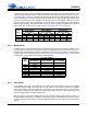
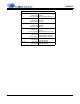
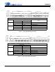
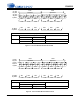
Table Of Contents
- 1. Characteristics and Specifications
- Specified Operating Conditions
- Absolute Maximum Ratings
- Analog Input Characteristics
- A/D Digital Filter Characteristics
- Analog Output Characteristics
- D/A Digital Filter Characteristics
- Switching Characteristics
- Switching Characteristics - Control Port - I²C™ Format
- Switching Characteristics - Control Port - SPI™ Format
- DC Electrical Characteristics
- Digital Interface Characteristics
- 2. Pin Descriptions
- 3. Typical Connection Diagram
- 4. Applications
- 4.1 Overview
- 4.2 Analog Inputs
- 4.3 Analog Outputs
- 4.4 S/PDIF Receiver
- 4.5 Clock Generation
- 4.6 Digital Interfaces
- 4.7 Control Port Description and Timing
- 4.8 Interrupts
- 4.9 Reset and Power-Up
- 4.10 Power Supply, Grounding, and PCB Layout
- 5. Register Quick Reference
- 6. Register Description
- Table 5. DAC De-Emphasis
- Table 6. Receiver De-Emphasis
- Table 7. Digital Interface Formats
- Table 8. ADC One-Line Mode
- Table 9. DAC One-Line Mode
- Table 10. RMCK Divider Settings
- Table 11. OMCK Frequency Settings
- Table 12. Master Clock Source Select
- Table 13. AES Format Detection
- Table 14. Receiver Clock Frequency Detection
- Table 15. Example Digital Volume Settings
- Table 16. ATAPI Decode
- Table 17. Example ADC Input Gain Settings
- Table 18. TXP Output Selection
- Table 19. Receiver Input Selection
- Table 20. Auxiliary Data Width Selection
- 7. Parameter Definitions
- 8. Appendix A: External Filters
- 9. Appendix B: S/PDIF Receiver
- 10. Appendix C: PLL Filter
- 11. Appendix D: External AES3-S/PDIF-IEC60958 Receiver Components
- 12. Appendix E: ADC Filter Plots
- Figure 34. Single-Speed Mode Stopband Rejection
- Figure 35. Single-Speed Mode Transition Band
- Figure 36. Single-Speed Mode Transition Band (Detail)
- Figure 37. Single-Speed Mode Passband Ripple
- Figure 38. Double-Speed Mode Stopband Rejection
- Figure 39. Double-Speed Mode Transition Band
- Figure 40. Double-Speed Mode Transition Band (Detail)
- Figure 41. Double-Speed Mode Passband Ripple
- Figure 42. Quad-Speed Mode Stopband Rejection
- Figure 43. Quad-Speed Mode Transition Band
- Figure 44. Quad-Speed Mode Transition Band (Detail)
- Figure 45. Quad-Speed Mode Passband Ripple
- 13. Appendix F: DAC Filter Plots
- Figure 46. Single-Speed (fast) Stopband Rejection
- Figure 47. Single-Speed (fast) Transition Band
- Figure 48. Single-Speed (fast) Transition Band (detail)
- Figure 49. Single-Speed (fast) Passband Ripple
- Figure 50. Single-Speed (slow) Stopband Rejection
- Figure 51. Single-Speed (slow) Transition Band
- Figure 52. Single-Speed (slow) Transition Band (detail)
- Figure 53. Single-Speed (slow) Passband Ripple
- Figure 54. Double-Speed (fast) Stopband Rejection
- Figure 55. Double-Speed (fast) Transition Band
- Figure 56. Double-Speed (fast) Transition Band (detail)
- Figure 57. Double-Speed (fast) Passband Ripple
- Figure 58. Double-Speed (slow) Stopband Rejection
- Figure 59. Double-Speed (slow) Transition Band
- Figure 60. Double-Speed (slow) Transition Band (detail)
- Figure 61. Double-Speed (slow) Passband Ripple
- Figure 62. Quad-Speed (fast) Stopband Rejection
- Figure 63. Quad-Speed (fast) Transition Band
- Figure 64. Quad-Speed (fast) Transition Band (detail)
- Figure 65. Quad-Speed (fast) Passband Ripple
- Figure 66. Quad-Speed (slow) Stopband Rejection
- Figure 67. Quad-Speed (slow) Transition Band
- Figure 68. Quad-Speed (slow) Transition Band (detail)
- Figure 69. Quad-Speed (slow) Passband Ripple
- 14. Package Dimensions
- 15. Ordering Information
- 16. References
- 17. Revision History
DS583F2 23
CS42516
4.4 S/PDIF Receiver
The CS42516 includes an S/PDIF digital audio receiver. The S/PDIF receiver accepts and decodes digital
audio data according to the IEC60958 (S/PDIF), and EIAJ CP-1201 interface standards. The receiver con-
sists of an 8:2 multiplexer input stage driven through pins RXP0 and RXP1/GPO1 - RXP7/GPO7, a PLL
based clock recovery circuit, and a decoder which separates the audio data from the channel status and
user data. A comprehensive buffering scheme provides read access to the channel status and user data.
External components are used to terminate and isolate the incoming data cables from the CS42516. These
components and required circuitry are detailed in the CDB42518.
4.4.1 8:2 S/PDIF Input Multiplexer
The CS42516 contains an 8:2 S/PDIF Input Multiplexer to accommodate up to eight channels of input dig-
ital audio data. Digital audio data is single-ended and input through the RXP0 and
RXP1/GPO1-RXP7/GPO7 pins. Any one of these inputs can be multiplexed to the input of the S/PDIF
receiver and to the S/PDIF output pin TXP.
When any portion of the multiplexer is implemented, unused RXP0 and RXPx/GPOx pins should be tied
to a 0.01uF capacitor to ground. The receiver multiplexer select line control is accessed through bits
RMUX2:0 in the Receiver Mode Control 2 register on page 63. The TXP multiplexer select line control is
accessed through bits TMUX2:0 in the same register. The multiplexer defaults to RXP0 for both functions.
4.4.2 Error Reporting and Hold Function
While decoding the incoming S/PDIF data stream, the CS42516 can identify several kinds of error, indi-
cated in the register “Receiver Errors (address 26h) (Read Only)” on page 67. See “Error Reporting and
Hold Function” on page 74 for more information.
4.4.3 Channel Status Data Handling
The first 2 bytes of the Channel Status block (C data) are decoded into the Receiver Channel Status reg-
ister (See “Receiver Channel Status (address 25h) (Read Only)” on page 66). See “Channel Status Data
Handling” on page 74 for more information.
4.4.4 User Data Handling
The incoming User (U) data is buffered in a user accessible buffer. If the U data bits have been encoded
as Q-channel subcode, the data is decoded and presented in 10 consecutive register locations, address
30h to 39h. The user can configure the Interrupt Mask Register to cause interrupts to indicate the decod-
ing of a new Q-channel block, which may be read through the control port. See “User (U) Data E Buffer
Access” on page 76 for more information.
4.4.5 Non-Audio Auto-Detection
A S/PDIF data stream may be used to convey non-audio data, thus it is important to know whether the
incoming data stream is digital PCM audio samples or not. This information is typically conveyed in chan-
nel status bit 1 (AUDIO
), which is extracted automatically by the CS42516. Certain non-audio sources,
however, such as AC-3
or MPEG encoders, may not adhere to this convention, and the bit may not be
properly set. See “Non-Audio Auto-Detection” on page 76 for more information including details for inter-
face format detection.