
User guide
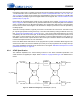
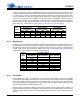
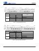
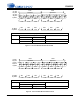
Table Of Contents
- 1. Characteristics and Specifications
- Specified Operating Conditions
- Absolute Maximum Ratings
- Analog Input Characteristics
- A/D Digital Filter Characteristics
- Analog Output Characteristics
- D/A Digital Filter Characteristics
- Switching Characteristics
- Switching Characteristics - Control Port - I²C™ Format
- Switching Characteristics - Control Port - SPI™ Format
- DC Electrical Characteristics
- Digital Interface Characteristics
- 2. Pin Descriptions
- 3. Typical Connection Diagram
- 4. Applications
- 4.1 Overview
- 4.2 Analog Inputs
- 4.3 Analog Outputs
- 4.4 S/PDIF Receiver
- 4.5 Clock Generation
- 4.6 Digital Interfaces
- 4.7 Control Port Description and Timing
- 4.8 Interrupts
- 4.9 Reset and Power-Up
- 4.10 Power Supply, Grounding, and PCB Layout
- 5. Register Quick Reference
- 6. Register Description
- Table 5. DAC De-Emphasis
- Table 6. Receiver De-Emphasis
- Table 7. Digital Interface Formats
- Table 8. ADC One-Line Mode
- Table 9. DAC One-Line Mode
- Table 10. RMCK Divider Settings
- Table 11. OMCK Frequency Settings
- Table 12. Master Clock Source Select
- Table 13. AES Format Detection
- Table 14. Receiver Clock Frequency Detection
- Table 15. Example Digital Volume Settings
- Table 16. ATAPI Decode
- Table 17. Example ADC Input Gain Settings
- Table 18. TXP Output Selection
- Table 19. Receiver Input Selection
- Table 20. Auxiliary Data Width Selection
- 7. Parameter Definitions
- 8. Appendix A: External Filters
- 9. Appendix B: S/PDIF Receiver
- 10. Appendix C: PLL Filter
- 11. Appendix D: External AES3-S/PDIF-IEC60958 Receiver Components
- 12. Appendix E: ADC Filter Plots
- Figure 34. Single-Speed Mode Stopband Rejection
- Figure 35. Single-Speed Mode Transition Band
- Figure 36. Single-Speed Mode Transition Band (Detail)
- Figure 37. Single-Speed Mode Passband Ripple
- Figure 38. Double-Speed Mode Stopband Rejection
- Figure 39. Double-Speed Mode Transition Band
- Figure 40. Double-Speed Mode Transition Band (Detail)
- Figure 41. Double-Speed Mode Passband Ripple
- Figure 42. Quad-Speed Mode Stopband Rejection
- Figure 43. Quad-Speed Mode Transition Band
- Figure 44. Quad-Speed Mode Transition Band (Detail)
- Figure 45. Quad-Speed Mode Passband Ripple
- 13. Appendix F: DAC Filter Plots
- Figure 46. Single-Speed (fast) Stopband Rejection
- Figure 47. Single-Speed (fast) Transition Band
- Figure 48. Single-Speed (fast) Transition Band (detail)
- Figure 49. Single-Speed (fast) Passband Ripple
- Figure 50. Single-Speed (slow) Stopband Rejection
- Figure 51. Single-Speed (slow) Transition Band
- Figure 52. Single-Speed (slow) Transition Band (detail)
- Figure 53. Single-Speed (slow) Passband Ripple
- Figure 54. Double-Speed (fast) Stopband Rejection
- Figure 55. Double-Speed (fast) Transition Band
- Figure 56. Double-Speed (fast) Transition Band (detail)
- Figure 57. Double-Speed (fast) Passband Ripple
- Figure 58. Double-Speed (slow) Stopband Rejection
- Figure 59. Double-Speed (slow) Transition Band
- Figure 60. Double-Speed (slow) Transition Band (detail)
- Figure 61. Double-Speed (slow) Passband Ripple
- Figure 62. Quad-Speed (fast) Stopband Rejection
- Figure 63. Quad-Speed (fast) Transition Band
- Figure 64. Quad-Speed (fast) Transition Band (detail)
- Figure 65. Quad-Speed (fast) Passband Ripple
- Figure 66. Quad-Speed (slow) Stopband Rejection
- Figure 67. Quad-Speed (slow) Transition Band
- Figure 68. Quad-Speed (slow) Transition Band (detail)
- Figure 69. Quad-Speed (slow) Passband Ripple
- 14. Package Dimensions
- 15. Ordering Information
- 16. References
- 17. Revision History
22 DS583F2
CS42516
4.3.3 Digital Volume and Mute Control
Each DAC’s output level is controlled via the Volume Control registers operating over the range of 0 to
-127 dB attenuation with 0.5 dB resolution. See “Volume Control (addresses 0Fh, 10h, 11h, 12h, 13h,
14h)” on page 58. Volume control changes are programmable to ramp in increments of 0.125 dB at the
rate controlled by the SZC[1:0] bits in the Digital Volume Control register. See “Volume Transition Control
(address 0Dh)” on page 56.
Each output can be independently muted via mute control bits in the register “Channel Mute (address
0Eh)” on page 58. When enabled, each XX_MUTE bit attenuates the corresponding DAC to its maximum
value (-127 dB). When the XX_MUTE bit is disabled, the corresponding DAC returns to the attenuation
level set in the Volume Control register. The attenuation is ramped up and down at the rate specified by
the SZC[1:0] bits.
The Mute Control pin, MUTEC, is typically connected to an external mute control circuit. The Mute Control
pin outputs high impedance during Power-Up or in Power-Down Mode by setting the PDN bit in the reg-
ister “Power Control (address 02h)” on page 46 to a ‘1’. Once out of Power-Down Mode, the pin can be
controlled by the user via the control port, or automatically asserted high when zero data is present on all
DAC inputs, or when serial port clock errors are present. To prevent large transients on the output, it is
desirable to mute the DAC outputs before the Mute Control pin is asserted. Please see the MUTEC pin
in the Pin Descriptions section for more information.
Each of the RXP1/GPO1-RXP7/GPO7 can be programmed to provide a hardware MUTE signal to indi-
vidual circuits. When not used as an S/PDIF input, each pin can be programmed as an output, with spe-
cific muting capabilities as defined by the function bits in the register “RXP/General-Purpose Pin Control
(addresses 29h to 2Fh)” on page 69.
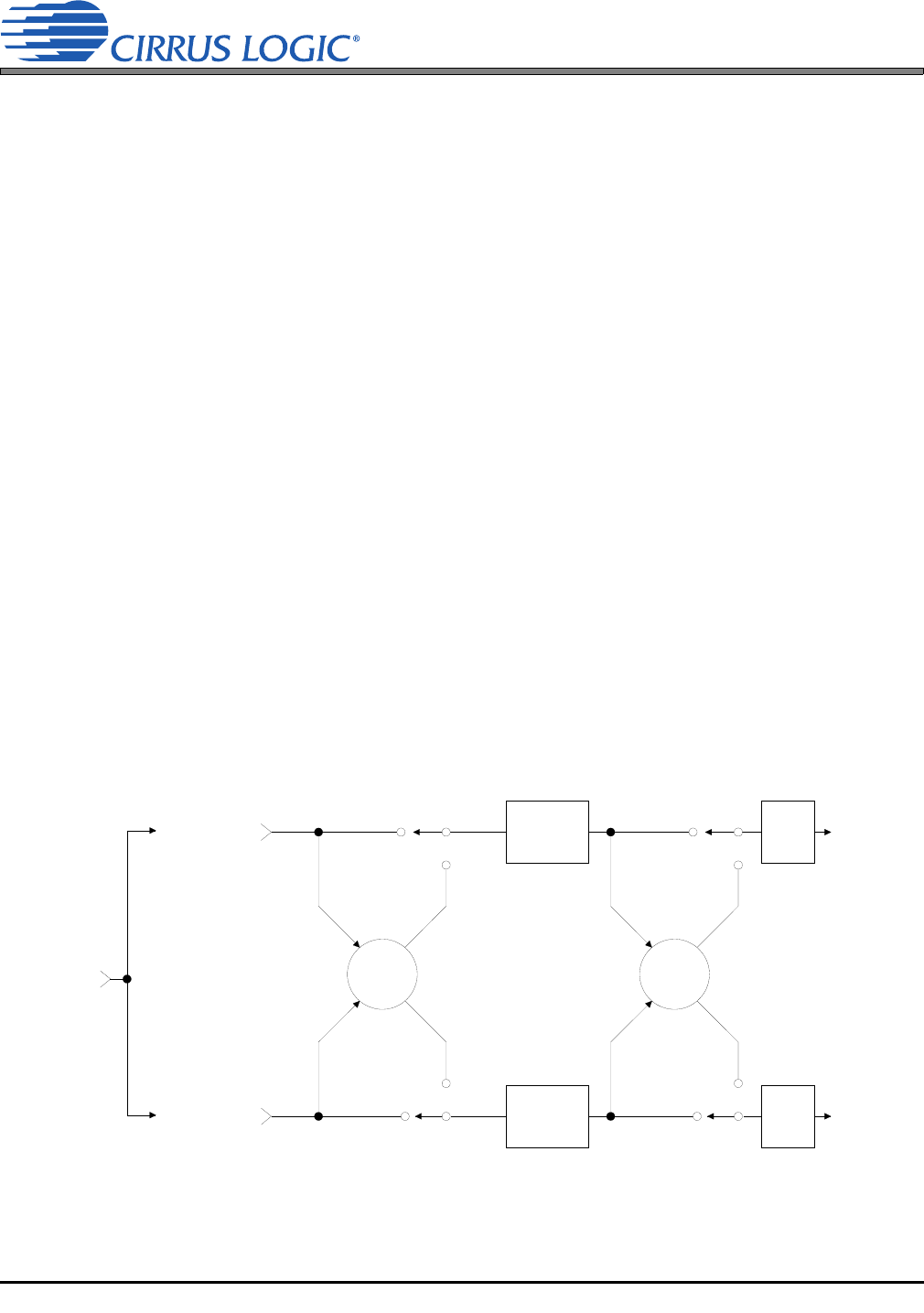
4.3.4 ATAPI Specification
The CS42516 implements the channel-mixing functions of the ATAPI CD-ROM specification. The
ATAPI functions are applied per A-B pair. Refer to Table 16 on page 60 and Figure 8 for additional infor-
mation.
A Channel
Volume
Control
AOUTAx
AOUTBx
Left Channel
Audio Data
Right Channel
Audio Data
BChannel
Volume
Control
MUTE
MUTE
CX_SDINx
Figure 8. ATAPI Block Diagram (x = channel pair 1, 2, or 3)