
User guide
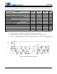
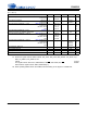
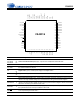
Table Of Contents
- 1. Characteristics and Specifications
- Specified Operating Conditions
- Absolute Maximum Ratings
- Analog Input Characteristics
- A/D Digital Filter Characteristics
- Analog Output Characteristics
- D/A Digital Filter Characteristics
- Switching Characteristics
- Switching Characteristics - Control Port - I²C™ Format
- Switching Characteristics - Control Port - SPI™ Format
- DC Electrical Characteristics
- Digital Interface Characteristics
- 2. Pin Descriptions
- 3. Typical Connection Diagram
- 4. Applications
- 4.1 Overview
- 4.2 Analog Inputs
- 4.3 Analog Outputs
- 4.4 S/PDIF Receiver
- 4.5 Clock Generation
- 4.6 Digital Interfaces
- 4.7 Control Port Description and Timing
- 4.8 Interrupts
- 4.9 Reset and Power-Up
- 4.10 Power Supply, Grounding, and PCB Layout
- 5. Register Quick Reference
- 6. Register Description
- Table 5. DAC De-Emphasis
- Table 6. Receiver De-Emphasis
- Table 7. Digital Interface Formats
- Table 8. ADC One-Line Mode
- Table 9. DAC One-Line Mode
- Table 10. RMCK Divider Settings
- Table 11. OMCK Frequency Settings
- Table 12. Master Clock Source Select
- Table 13. AES Format Detection
- Table 14. Receiver Clock Frequency Detection
- Table 15. Example Digital Volume Settings
- Table 16. ATAPI Decode
- Table 17. Example ADC Input Gain Settings
- Table 18. TXP Output Selection
- Table 19. Receiver Input Selection
- Table 20. Auxiliary Data Width Selection
- 7. Parameter Definitions
- 8. Appendix A: External Filters
- 9. Appendix B: S/PDIF Receiver
- 10. Appendix C: PLL Filter
- 11. Appendix D: External AES3-S/PDIF-IEC60958 Receiver Components
- 12. Appendix E: ADC Filter Plots
- Figure 34. Single-Speed Mode Stopband Rejection
- Figure 35. Single-Speed Mode Transition Band
- Figure 36. Single-Speed Mode Transition Band (Detail)
- Figure 37. Single-Speed Mode Passband Ripple
- Figure 38. Double-Speed Mode Stopband Rejection
- Figure 39. Double-Speed Mode Transition Band
- Figure 40. Double-Speed Mode Transition Band (Detail)
- Figure 41. Double-Speed Mode Passband Ripple
- Figure 42. Quad-Speed Mode Stopband Rejection
- Figure 43. Quad-Speed Mode Transition Band
- Figure 44. Quad-Speed Mode Transition Band (Detail)
- Figure 45. Quad-Speed Mode Passband Ripple
- 13. Appendix F: DAC Filter Plots
- Figure 46. Single-Speed (fast) Stopband Rejection
- Figure 47. Single-Speed (fast) Transition Band
- Figure 48. Single-Speed (fast) Transition Band (detail)
- Figure 49. Single-Speed (fast) Passband Ripple
- Figure 50. Single-Speed (slow) Stopband Rejection
- Figure 51. Single-Speed (slow) Transition Band
- Figure 52. Single-Speed (slow) Transition Band (detail)
- Figure 53. Single-Speed (slow) Passband Ripple
- Figure 54. Double-Speed (fast) Stopband Rejection
- Figure 55. Double-Speed (fast) Transition Band
- Figure 56. Double-Speed (fast) Transition Band (detail)
- Figure 57. Double-Speed (fast) Passband Ripple
- Figure 58. Double-Speed (slow) Stopband Rejection
- Figure 59. Double-Speed (slow) Transition Band
- Figure 60. Double-Speed (slow) Transition Band (detail)
- Figure 61. Double-Speed (slow) Passband Ripple
- Figure 62. Quad-Speed (fast) Stopband Rejection
- Figure 63. Quad-Speed (fast) Transition Band
- Figure 64. Quad-Speed (fast) Transition Band (detail)
- Figure 65. Quad-Speed (fast) Passband Ripple
- Figure 66. Quad-Speed (slow) Stopband Rejection
- Figure 67. Quad-Speed (slow) Transition Band
- Figure 68. Quad-Speed (slow) Transition Band (detail)
- Figure 69. Quad-Speed (slow) Passband Ripple
- 14. Package Dimensions
- 15. Ordering Information
- 16. References
- 17. Revision History
20 DS583F2
CS42516
4. APPLICATIONS
4.1 Overview
The CS42516 is a highly integrated mixed-signal 24-bit audio codec comprised of 2 analog-to-digital con-
verters (ADC), implemented using multi-bit delta-sigma techniques, 6 digital-to-analog converters (DAC)
and a 192 kHz digital audio S/PDIF receiver. Other functions integrated within the codec include indepen-
dent digital volume controls for each DAC, digital de-emphasis filters for DAC and S/PDIF, digital gain con-
trol for ADC channels, ADC high-pass filters, an on-chip voltage reference, and an 8:2 mux for S/PDIF
sources. All serial data is transmitted through two configurable serial audio interfaces with standard serial
interface support as well as enhanced one-line modes of operation, allowing up to 6 channels of serial audio
data on one data line. All functions are configured through a serial control port operable in SPI mode or in
I²C mode. 5 show the recommended connections for the CS42516.
The CS42516 operates in one of three oversampling modes based on the input sample rate. Mode selection
is determined by the FM bits in register “Functional Mode (address 03h)” on page 47. Single-Speed Mode
(SSM) supports input sample rates up to 50 kHz and uses a 128x oversampling ratio. Double-Speed Mode
(DSM) supports input sample rates up to 100 kHz and uses an oversampling ratio of 64x. Quad-Speed
Mode (QSM) supports input sample rates up to 192 kHz and uses an oversampling ratio of 32x.
Using the receiver clock recovery PLL, a low-jitter clock is recovered from the incoming S/PDIF data stream.
The recovered clock or an externally supplied clock attached to the OMCK pin can be used as the System
Clock.
4.2 Analog Inputs
4.2.1 Line-Level Inputs
AINR+, AINR-, AINL+, and AINL- are the line-level differential analog inputs. The analog signal must be
externally biased to VQ, approximately 2.7 V, before being applied to these inputs. The level of the signal
can be adjusted for the left and right ADC independently through the ADC Left and Right Channel Gain
Control Registers on page 61. The ADC output data is in two’s complement binary format. For inputs
above positive full scale or below negative full scale, the ADC will output 7FFFFFH or 800000H, respec-
tively and cause the ADC Overflow bit in the register “Interrupt Status (address 20h) (Read Only)” on
page 63 to be set to a ‘1’. The RXP/GPO pins may also be configured to indicate an overflow condition
has occurred in the ADC. See “RXP/General-Purpose Pin Control (addresses 29h to 2Fh)” on page 69
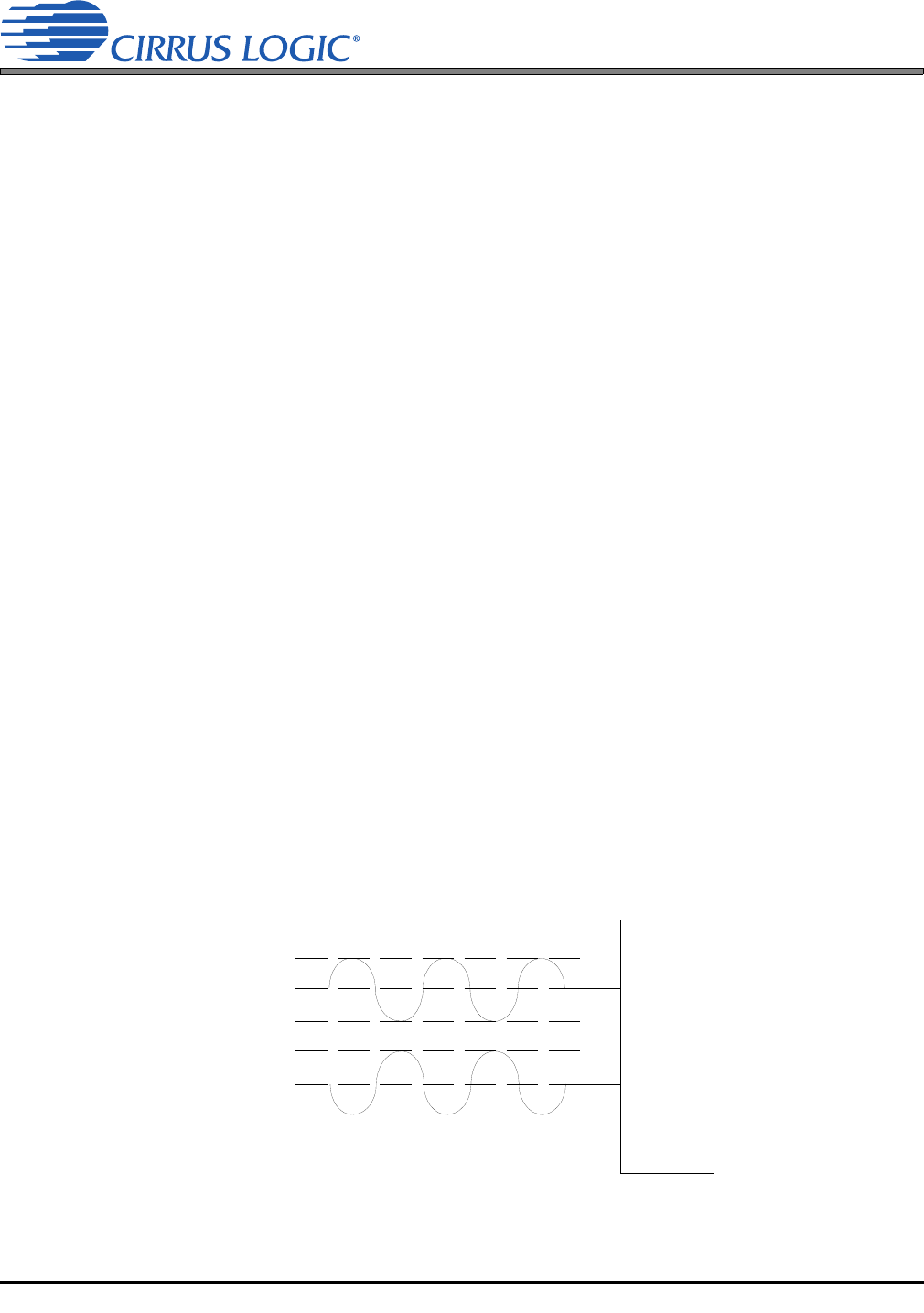
for proper configuration. Figure 6 shows the full-scale analog input levels. See “ADC Input Filter” on
page 73 for a recommended input buffer.
AIN+
AIN-
Full-Scale Input Level= (AIN+) - (AIN-)= 5.6 Vpp
4.1 V
2.7 V
1.3 V
4.1 V
2.7 V
1.3 V
Figure 6. Full-Scale Analog Input