
User guide
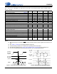
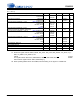
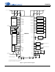
Table Of Contents
- 1. Characteristics and Specifications
- Specified Operating Conditions
- Absolute Maximum Ratings
- Analog Input Characteristics
- A/D Digital Filter Characteristics
- Analog Output Characteristics
- D/A Digital Filter Characteristics
- Switching Characteristics
- Switching Characteristics - Control Port - I²C™ Format
- Switching Characteristics - Control Port - SPI™ Format
- DC Electrical Characteristics
- Digital Interface Characteristics
- 2. Pin Descriptions
- 3. Typical Connection Diagram
- 4. Applications
- 4.1 Overview
- 4.2 Analog Inputs
- 4.3 Analog Outputs
- 4.4 S/PDIF Receiver
- 4.5 Clock Generation
- 4.6 Digital Interfaces
- 4.7 Control Port Description and Timing
- 4.8 Interrupts
- 4.9 Reset and Power-Up
- 4.10 Power Supply, Grounding, and PCB Layout
- 5. Register Quick Reference
- 6. Register Description
- Table 5. DAC De-Emphasis
- Table 6. Receiver De-Emphasis
- Table 7. Digital Interface Formats
- Table 8. ADC One-Line Mode
- Table 9. DAC One-Line Mode
- Table 10. RMCK Divider Settings
- Table 11. OMCK Frequency Settings
- Table 12. Master Clock Source Select
- Table 13. AES Format Detection
- Table 14. Receiver Clock Frequency Detection
- Table 15. Example Digital Volume Settings
- Table 16. ATAPI Decode
- Table 17. Example ADC Input Gain Settings
- Table 18. TXP Output Selection
- Table 19. Receiver Input Selection
- Table 20. Auxiliary Data Width Selection
- 7. Parameter Definitions
- 8. Appendix A: External Filters
- 9. Appendix B: S/PDIF Receiver
- 10. Appendix C: PLL Filter
- 11. Appendix D: External AES3-S/PDIF-IEC60958 Receiver Components
- 12. Appendix E: ADC Filter Plots
- Figure 34. Single-Speed Mode Stopband Rejection
- Figure 35. Single-Speed Mode Transition Band
- Figure 36. Single-Speed Mode Transition Band (Detail)
- Figure 37. Single-Speed Mode Passband Ripple
- Figure 38. Double-Speed Mode Stopband Rejection
- Figure 39. Double-Speed Mode Transition Band
- Figure 40. Double-Speed Mode Transition Band (Detail)
- Figure 41. Double-Speed Mode Passband Ripple
- Figure 42. Quad-Speed Mode Stopband Rejection
- Figure 43. Quad-Speed Mode Transition Band
- Figure 44. Quad-Speed Mode Transition Band (Detail)
- Figure 45. Quad-Speed Mode Passband Ripple
- 13. Appendix F: DAC Filter Plots
- Figure 46. Single-Speed (fast) Stopband Rejection
- Figure 47. Single-Speed (fast) Transition Band
- Figure 48. Single-Speed (fast) Transition Band (detail)
- Figure 49. Single-Speed (fast) Passband Ripple
- Figure 50. Single-Speed (slow) Stopband Rejection
- Figure 51. Single-Speed (slow) Transition Band
- Figure 52. Single-Speed (slow) Transition Band (detail)
- Figure 53. Single-Speed (slow) Passband Ripple
- Figure 54. Double-Speed (fast) Stopband Rejection
- Figure 55. Double-Speed (fast) Transition Band
- Figure 56. Double-Speed (fast) Transition Band (detail)
- Figure 57. Double-Speed (fast) Passband Ripple
- Figure 58. Double-Speed (slow) Stopband Rejection
- Figure 59. Double-Speed (slow) Transition Band
- Figure 60. Double-Speed (slow) Transition Band (detail)
- Figure 61. Double-Speed (slow) Passband Ripple
- Figure 62. Quad-Speed (fast) Stopband Rejection
- Figure 63. Quad-Speed (fast) Transition Band
- Figure 64. Quad-Speed (fast) Transition Band (detail)
- Figure 65. Quad-Speed (fast) Passband Ripple
- Figure 66. Quad-Speed (slow) Stopband Rejection
- Figure 67. Quad-Speed (slow) Transition Band
- Figure 68. Quad-Speed (slow) Transition Band (detail)
- Figure 69. Quad-Speed (slow) Passband Ripple
- 14. Package Dimensions
- 15. Ordering Information
- 16. References
- 17. Revision History
DS583F2 19
CS42516
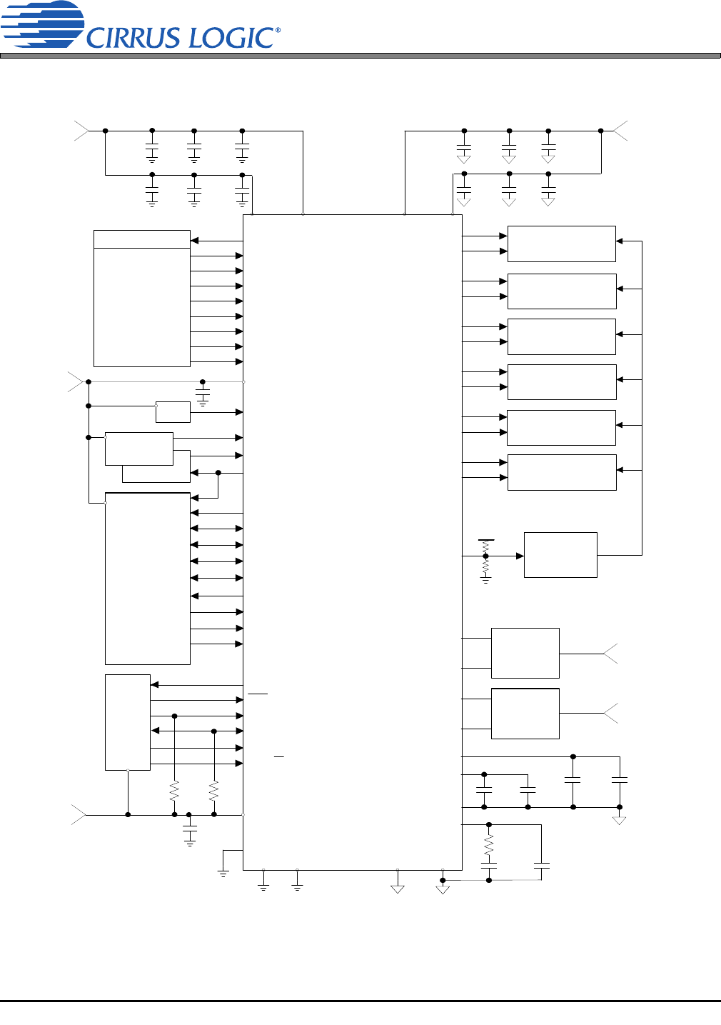
3. TYPICAL CONNECTION DIAGRAM
VD
AOUTA1+
24
0.1 µF
+
10 µF
100 µF
0.1 µF
+
+
17
18
VQ
FILT+
36
37
0.1 µF
4.7 µF
VA
+
10 µF
51
AOUTA1-
AOUTB1+
35
34
AOUTB1-
AOUTA2+
32
33
AOUTA2-
AOUTB2+
31
30
AOUTB2-
AOUTA3+
28
29
AOUTA3-
AOUTB3+
27
26
AOUTB3-
MUTEC
38
25
DGND
DGND
5
REFGND
19
41
4
VAVD
0.1 µF
AGNDAGND
52 40
LPFLT
39
AINL+
AINL-
AINR+
AINR-
15
16
14
13
Connect DGND and AGND at single point near Codec
0.01 µF
0.1 µF
+
10 µF
+5 V
0.01 µF
0.01 µF
+3.3 V to +5 V
+
10 µF
0.1 µF 0.01 µF
VLS
0.1 µF
+2.5 V
to +5 V
53
VLC
0.1 µF
+1.8 V
to +5 V
6
3
60
59
1
64
61
2
63
8
7
SCL/CCLK
SDA/CDOUT
AD1/CDIN
RST
12
9
OMCK
CX_SDIN1
SAI_LRCK
SAI_SCLK
CX_SDIN3
CX_SDIN2
CX_LRCK
CX_SCLK
AD0/CS
10
INT
11
Digital Audio
Processor
Micro-
Controller
55
RMCK
58
ADCIN1
57
ADCIN2
CS5361
A/D Converter
CS5361
A/D Converter
56
CX_SDOUT
54
SAI_SDOUT
48
46
49
44
45
47
RXP0
RXP1/GPO1
S/PDIF
Interface
50
TXP
Driver
Up to 8
Sources
43
RXP2/GPO2
RXP3/GPO3
RXP4/GPO4
RXP5/GPO5
RXP6/GPO6
RXP7/GPO7
42
OSC
Analog Output Buffer
2
and
Mute Circuit (optional)
Mute
Drive
(optional)
2700 pF*
2700 pF*
Left Analog Input
Right Analog Input
Analog
Input
Buffer
1
Analog
Input
Buffer
1
+VA
*
* Pull up or down as
required on startup if the
M ute Control is u sed.
*
Analog Output Buffer
2
and
Mute Circuit (optional)
Analog Output Buffer
2
and
Mute Circuit (optional)
Analog Output Buffer
2
and
Mute Circuit (optional)
Analog Output Buffer
2
and
Mute Circuit (optional)
Analog Output Buffer
2
and
Mute Circuit (optional)
2 k 2 k
** **
CFILT
3
RFILT
3
CRIP
3
** Resistors are required for
I
2
C control port operation
1. See the ADC Input Filter section in the Appendix.
2. See the DAC Output Filter section in the Appendix.
3. See the PLL Filter section in the Appendix.
62
TEST
Figure 5. Typical Connection Diagram
CS42516