
User guide
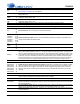
Table Of Contents
- 1. Characteristics and Specifications
- Specified Operating Conditions
- Absolute Maximum Ratings
- Analog Input Characteristics
- A/D Digital Filter Characteristics
- Analog Output Characteristics
- D/A Digital Filter Characteristics
- Switching Characteristics
- Switching Characteristics - Control Port - I²C™ Format
- Switching Characteristics - Control Port - SPI™ Format
- DC Electrical Characteristics
- Digital Interface Characteristics
- 2. Pin Descriptions
- 3. Typical Connection Diagram
- 4. Applications
- 4.1 Overview
- 4.2 Analog Inputs
- 4.3 Analog Outputs
- 4.4 S/PDIF Receiver
- 4.5 Clock Generation
- 4.6 Digital Interfaces
- 4.7 Control Port Description and Timing
- 4.8 Interrupts
- 4.9 Reset and Power-Up
- 4.10 Power Supply, Grounding, and PCB Layout
- 5. Register Quick Reference
- 6. Register Description
- Table 5. DAC De-Emphasis
- Table 6. Receiver De-Emphasis
- Table 7. Digital Interface Formats
- Table 8. ADC One-Line Mode
- Table 9. DAC One-Line Mode
- Table 10. RMCK Divider Settings
- Table 11. OMCK Frequency Settings
- Table 12. Master Clock Source Select
- Table 13. AES Format Detection
- Table 14. Receiver Clock Frequency Detection
- Table 15. Example Digital Volume Settings
- Table 16. ATAPI Decode
- Table 17. Example ADC Input Gain Settings
- Table 18. TXP Output Selection
- Table 19. Receiver Input Selection
- Table 20. Auxiliary Data Width Selection
- 7. Parameter Definitions
- 8. Appendix A: External Filters
- 9. Appendix B: S/PDIF Receiver
- 10. Appendix C: PLL Filter
- 11. Appendix D: External AES3-S/PDIF-IEC60958 Receiver Components
- 12. Appendix E: ADC Filter Plots
- Figure 34. Single-Speed Mode Stopband Rejection
- Figure 35. Single-Speed Mode Transition Band
- Figure 36. Single-Speed Mode Transition Band (Detail)
- Figure 37. Single-Speed Mode Passband Ripple
- Figure 38. Double-Speed Mode Stopband Rejection
- Figure 39. Double-Speed Mode Transition Band
- Figure 40. Double-Speed Mode Transition Band (Detail)
- Figure 41. Double-Speed Mode Passband Ripple
- Figure 42. Quad-Speed Mode Stopband Rejection
- Figure 43. Quad-Speed Mode Transition Band
- Figure 44. Quad-Speed Mode Transition Band (Detail)
- Figure 45. Quad-Speed Mode Passband Ripple
- 13. Appendix F: DAC Filter Plots
- Figure 46. Single-Speed (fast) Stopband Rejection
- Figure 47. Single-Speed (fast) Transition Band
- Figure 48. Single-Speed (fast) Transition Band (detail)
- Figure 49. Single-Speed (fast) Passband Ripple
- Figure 50. Single-Speed (slow) Stopband Rejection
- Figure 51. Single-Speed (slow) Transition Band
- Figure 52. Single-Speed (slow) Transition Band (detail)
- Figure 53. Single-Speed (slow) Passband Ripple
- Figure 54. Double-Speed (fast) Stopband Rejection
- Figure 55. Double-Speed (fast) Transition Band
- Figure 56. Double-Speed (fast) Transition Band (detail)
- Figure 57. Double-Speed (fast) Passband Ripple
- Figure 58. Double-Speed (slow) Stopband Rejection
- Figure 59. Double-Speed (slow) Transition Band
- Figure 60. Double-Speed (slow) Transition Band (detail)
- Figure 61. Double-Speed (slow) Passband Ripple
- Figure 62. Quad-Speed (fast) Stopband Rejection
- Figure 63. Quad-Speed (fast) Transition Band
- Figure 64. Quad-Speed (fast) Transition Band (detail)
- Figure 65. Quad-Speed (fast) Passband Ripple
- Figure 66. Quad-Speed (slow) Stopband Rejection
- Figure 67. Quad-Speed (slow) Transition Band
- Figure 68. Quad-Speed (slow) Transition Band (detail)
- Figure 69. Quad-Speed (slow) Passband Ripple
- 14. Package Dimensions
- 15. Ordering Information
- 16. References
- 17. Revision History
DS583F2 17
CS42516
INT
11
Interrupt (Output) - The CS42516 will generate an interrupt condition as per the Interrupt Mask register.
See “Interrupts” on page 39 for more details.
RST
12
Reset (Input) - The device enters a low power mode and all internal registers are reset to their default
settings when low.
AINR-
AINR+
13
14
Differential Right Channel Analog Input (Input) - Signals are presented differentially to the delta-sigma
modulators via the AINR+/- pins.
AINL+
AINL-
15
16
Differential Left Channel Analog Input (Input) - Signals are presented differentially to the delta-sigma
modulators via the AINL+/- pins.
VQ
17
Quiescent Voltage (Output) - Filter connection for internal quiescent reference voltage.
FILT+
18
Positive Voltage Reference (Output) - Positive reference voltage for the internal sampling circuits.
REFGND
19
Reference Ground (Input) - Ground reference for the internal sampling circuits.
NC
20
21
22
23
No Connect Pins - Do not make any connection to these pins.
AOUTA1 +,-
AOUTB1 +,-
AOUTA2 +,-
AOUTB2 +,-
AOUTA3 +,-
AOUTB3 +,-
36,37
35,34
32,33
31,30
28,29
27,26
Differential Analog Output (Output) - The full-scale differential analog output level is specified in the
Analog Characteristics specification table.
VA
VARX
24
41
Analog Power (Input) - Positive power supply for the analog section.
AGND
25
40
Analog Ground (Input) - Ground reference. Should be connected to analog ground.
MUTEC
38
Mute Control (Output) - The Mute Control pin outputs high impedance following an initial power-on con-
dition or whenever the PDN bit is set to a ‘1’, forcing the codec into power-down mode. The signal will
remain in a high impedance state as long as the part is in power-down mode. The Mute Control pin goes
to the selected “active” state during reset, muting, or if the master clock to left/right clock frequency ratio
is incorrect. This pin is intended to be used as a control for external mute circuits to prevent the clicks
and pops that can occur in any single supply system. The use of external mute circuits are not manda-
tory but may be desired for designs requiring the absolute minimum in extraneous clicks and pops.
LPFLT
39
PLL Loop Filter (Output) - An RC network should be connected between this pin and ground.
RXP7/GPO7
RXP6/GPO6
RXP5/GPO5
RXP4/GPO4
RXP3/GPO3
RXP2/GPO2
RXP1/GPO1
42
43
44
45
46
47
48
S/PDIF Receiver Input/ General Purpose Output (Input/Output) - Receiver inputs for S/PDIF encoded
data. The CS42516 has an internal 8:2 multiplexer to select the active receiver port, according to the
Receiver Mode Control 2 register. These pins can also be configured as general purpose output pins,
ADC Overflow indicators or Mute Control outputs according to the RXP/General Purpose Pin Control
registers.
RXP0
49
S/PDIF Receiver Input (Input) - Dedicated receiver input for S/PDIF encoded data.
TXP
50
S/PDIF Transmitter Output (Output) - S/PDIF encoded data output, mapped directly from one of the
receiver inputs as indicated by the Receiver Mode Control 2 register.
VLS
53
Serial Port Interface Power (Input) - Determines the required signal level for the serial port interfaces.
SAI_SDOUT
54
Serial Audio Interface Serial Data Output (Output) - Output for two’s complement serial audio PCM
data from the S/PDIF incoming stream. This pin can also be configured to transmit the output of the inter-
nal and external ADCs.
RMCK
55
Recovered Master Clock (Output) - Recovered master clock output from the External Clock Reference
(OMCK, pin 59) or the PLL which is locked to the incoming S/PDIF stream or CX_LRCK.
CX_SDOUT
56
CODEC Serial Data Output (Output) - Output for two’s complement serial audio data from the internal
and external ADCs.