
User guide
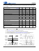
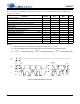
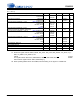
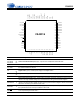
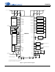
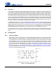
Table Of Contents
- 1. Characteristics and Specifications
- Specified Operating Conditions
- Absolute Maximum Ratings
- Analog Input Characteristics
- A/D Digital Filter Characteristics
- Analog Output Characteristics
- D/A Digital Filter Characteristics
- Switching Characteristics
- Switching Characteristics - Control Port - I²C™ Format
- Switching Characteristics - Control Port - SPI™ Format
- DC Electrical Characteristics
- Digital Interface Characteristics
- 2. Pin Descriptions
- 3. Typical Connection Diagram
- 4. Applications
- 4.1 Overview
- 4.2 Analog Inputs
- 4.3 Analog Outputs
- 4.4 S/PDIF Receiver
- 4.5 Clock Generation
- 4.6 Digital Interfaces
- 4.7 Control Port Description and Timing
- 4.8 Interrupts
- 4.9 Reset and Power-Up
- 4.10 Power Supply, Grounding, and PCB Layout
- 5. Register Quick Reference
- 6. Register Description
- Table 5. DAC De-Emphasis
- Table 6. Receiver De-Emphasis
- Table 7. Digital Interface Formats
- Table 8. ADC One-Line Mode
- Table 9. DAC One-Line Mode
- Table 10. RMCK Divider Settings
- Table 11. OMCK Frequency Settings
- Table 12. Master Clock Source Select
- Table 13. AES Format Detection
- Table 14. Receiver Clock Frequency Detection
- Table 15. Example Digital Volume Settings
- Table 16. ATAPI Decode
- Table 17. Example ADC Input Gain Settings
- Table 18. TXP Output Selection
- Table 19. Receiver Input Selection
- Table 20. Auxiliary Data Width Selection
- 7. Parameter Definitions
- 8. Appendix A: External Filters
- 9. Appendix B: S/PDIF Receiver
- 10. Appendix C: PLL Filter
- 11. Appendix D: External AES3-S/PDIF-IEC60958 Receiver Components
- 12. Appendix E: ADC Filter Plots
- Figure 34. Single-Speed Mode Stopband Rejection
- Figure 35. Single-Speed Mode Transition Band
- Figure 36. Single-Speed Mode Transition Band (Detail)
- Figure 37. Single-Speed Mode Passband Ripple
- Figure 38. Double-Speed Mode Stopband Rejection
- Figure 39. Double-Speed Mode Transition Band
- Figure 40. Double-Speed Mode Transition Band (Detail)
- Figure 41. Double-Speed Mode Passband Ripple
- Figure 42. Quad-Speed Mode Stopband Rejection
- Figure 43. Quad-Speed Mode Transition Band
- Figure 44. Quad-Speed Mode Transition Band (Detail)
- Figure 45. Quad-Speed Mode Passband Ripple
- 13. Appendix F: DAC Filter Plots
- Figure 46. Single-Speed (fast) Stopband Rejection
- Figure 47. Single-Speed (fast) Transition Band
- Figure 48. Single-Speed (fast) Transition Band (detail)
- Figure 49. Single-Speed (fast) Passband Ripple
- Figure 50. Single-Speed (slow) Stopband Rejection
- Figure 51. Single-Speed (slow) Transition Band
- Figure 52. Single-Speed (slow) Transition Band (detail)
- Figure 53. Single-Speed (slow) Passband Ripple
- Figure 54. Double-Speed (fast) Stopband Rejection
- Figure 55. Double-Speed (fast) Transition Band
- Figure 56. Double-Speed (fast) Transition Band (detail)
- Figure 57. Double-Speed (fast) Passband Ripple
- Figure 58. Double-Speed (slow) Stopband Rejection
- Figure 59. Double-Speed (slow) Transition Band
- Figure 60. Double-Speed (slow) Transition Band (detail)
- Figure 61. Double-Speed (slow) Passband Ripple
- Figure 62. Quad-Speed (fast) Stopband Rejection
- Figure 63. Quad-Speed (fast) Transition Band
- Figure 64. Quad-Speed (fast) Transition Band (detail)
- Figure 65. Quad-Speed (fast) Passband Ripple
- Figure 66. Quad-Speed (slow) Stopband Rejection
- Figure 67. Quad-Speed (slow) Transition Band
- Figure 68. Quad-Speed (slow) Transition Band (detail)
- Figure 69. Quad-Speed (slow) Passband Ripple
- 14. Package Dimensions
- 15. Ordering Information
- 16. References
- 17. Revision History
12 DS583F2
CS42516
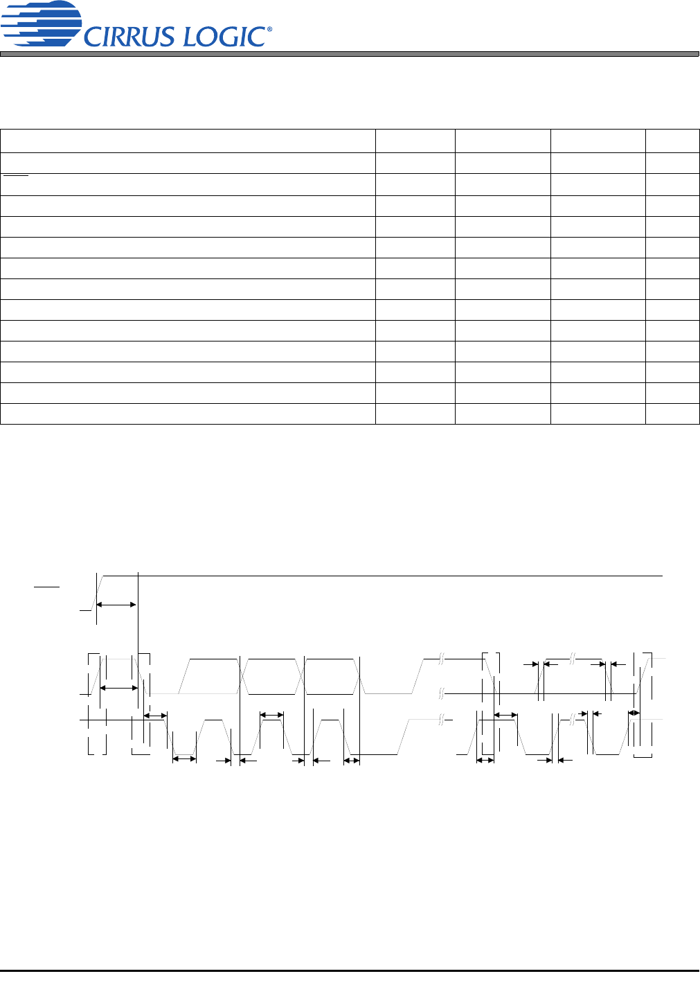
SWITCHING CHARACTERISTICS - CONTROL PORT - I²C™ FORMAT
(T
A
= -10 to +70° C; VA=VARX = 5 V, VD =VLS= 3.3 V; VLC = 1.8 V to 5.25 V; Inputs: Logic 0 = DGND, Logic
1=VLC, C
L
=30pF)
Notes:
17. Data must be held for sufficient time to bridge the transition time, t
fc
, of SCL.
18. The acknowledge delay is based on MCLK and can limit the maximum transaction speed.
19. for Single-Speed Mode, for Double-Speed Mode, for Quad-Speed Mode
Parameter Symbol Min Max Unit
SCL Clock Frequency
f
scl
- 100 kHz
RST
Rising Edge to Start
t
irs
500 - ns
Bus Free Time Between Transmissions
t
buf
4.7 - µs
Start Condition Hold Time (prior to first clock pulse)
t
hdst
4.0 - µs
Clock Low time
t
low
4.7 - µs
Clock High Time
t
high
4.0 - µs
Setup Time for Repeated Start Condition
t
sust
4.7 - µs
SDA Hold Time from SCL Falling (Note 17)
t
hdd
0-µs
SDA Setup time to SCL Rising
t
sud
250 - ns
Rise Time of SCL and SDA
t
rc
-1µs
Fall Time SCL and SDA
t
fc
- 300 ns
Setup Time for Stop Condition
t
susp
4.7 - µs
Acknowledge Delay from SCL Falling (Note 18)
t
ack
- (Note 19) ns
15
256 Fs
---------------------
15
128 Fs
---------------------
15
64 Fs
------------------
t
buf
t
hdst
t
low
t
hdd
t
high
t
sud
Stop Start
SDA
SCL
t
irs
RST
t
hdst
t
rc
t
fc
t
sust
t
susp
Start
Stop
Repeated
t
rd
t
fd
t
ack
Figure 3. Control Port Timing - I²C Format