
User Manual


DS656F3 43
CS4245
6.2.4 Power-Down DAC (Bit 1)
Function:
The DAC pair will remain in a reset state whenever this bit is set.
6.2.5 Power-Down Device (Bit 0)
Function:
The device will enter a low-power state whenever this bit is set. The power-down bit is set by default and
must be cleared before normal operation can occur. The contents of the control registers are retained
when the device is in power-down.
6.3 DAC Control - Address 03h
6.3.1 DAC Functional Mode (Bits 7:6)
Function:
Selects the required range of input sample rates.
6.3.2 DAC Digital Interface Format (Bits 5:4)
Function:
The required relationship between LRCK, SCLK and SDIN for the DAC is defined by the DAC Digital In-
terface Format and the options are detailed in Table 8 and Figures 7-9.
6.3.3 Mute DAC (Bit 2)
Function:
The DAC outputs will mute and the MUTEC
pin will become active when this bit is set. Though this bit is
active high, it should be noted that the MUTEC
pin is active low. The common mode voltage on the outputs
will be retained when this bit is set. The muting function is effected, similar to attenuation changes, by the
DACSoft and DACZero bits in the DAC Control 2 register.
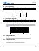
76543210
DAC_FM1 DAC_FM0 DAC_DIF1 DAC_DIF0 Reserved MuteDAC DeEmph DAC_M/S
DAC_FM1 DAC_FM0 Mode
0 0 Single-Speed Mode: 4 to 50 kHz sample rates
0 1 Double-Speed Mode: 50 to 100 kHz sample rates
1 0 Quad-Speed Mode: 100 to 200 kHz sample rates
11Reserved
Table 7. Functional Mode Selection
DAC_DIF1 DAC_DIF0 Description Format Figure
0 0 Left Justified, up to 24-bit data (default) 0 7
0 1 I²S, up to 24-bit data 1 8
1 0 Right-Justified, 16-bit Data 2 9
1 1 Right-Justified, 24-bit Data 3 9
Table 8. DAC Digital Interface Formats