
User Manual


32 DS656F3
CS4245
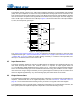
4.2.3 Master Mode
As a clock master, LRCK and SCLK will operate as outputs. The two serial ports may be independently
placed into Master or Slave mode. Each LRCK and SCLK is internally derived from its respective MCLK
with LRCK equal to Fs and SCLK equal to 64 x Fs as shown in Figure 13.
4.2.4 Slave Mode
In Slave Mode, SCLK and LRCK operate as inputs. Each serial port may be independently placed into
Slave Mode. The Left/Right clock signal must be equal to the sample rate, Fs. If operating in Asynchro-
nous Mode, LRCK1 must be synchronously derived from MCLK1 and LRCK2 must be synchronously de-
rived from MCLK2. If operating in Synchronous Mode, LRCK1, and LRCK2 must be synchronously
derived from MCLK1. For more information on Synchronous and Asynchronous Modes, see “Synchro-
nous / Asynchronous Mode” on page 30.
For each serial port, the serial bit clock must be equal to 128x, 64x, 48x or 32x Fs, depending on the de-
sired speed mode. If operating in Asynchronous Mode, the serial bit clock SCLK1 must be synchronously
derived from MCLK1 and SCLK2 must be synchronously derived from MCLK2. If operating in Synchro-
nous Mode, SCLK1, and SCLK2 must be synchronously derived from MCLK1. Refer to Table 4 for re-
quired serial bit clock to Left/Right clock ratios.
4.3 High-Pass Filter and DC Offset Calibration
When using operational amplifiers in the input circuitry driving the CS4245, a small DC offset may be driven
into the A/D converter. The CS4245 includes a high-pass filter after the decimator to remove any DC offset
which could result in recording a DC level, possibly yielding clicks when switching between devices in a mul-
tichannel system.
Single-Speed Double-Speed Quad-Speed
SCLK/LRCK Ratio 32x, 48x, 64x, 128x 32x, 48x, 64x 32x, 48x, 64x
Table 4. Slave Mode Serial Bit Clock Ratios
÷256
÷128
÷64
÷4
÷2
÷1
00
01
10
00
01
10
LRCK1
SCLK1
000
001
010
÷1
÷1.5
÷2
011
100
÷3
÷4
MCLK1
÷256
÷128
÷64
÷4
÷2
÷1
00
01
10
00
01
10
000
001
010
÷1
÷1.5
÷2
011
100
÷3
÷4
MCLK2
LRCK2
SCLK2
0
1
DAC_FM Bits
ADC_FM Bits
ASynch Bit
MCLK1 Freq Bits
MCLK2 Freq Bits
Figure 13. Master Mode Clocking