
User Manual


DS656F3 11
CS4245
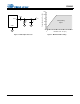
6. Guaranteed by design. See Figure 2. R
L
and C
L
reflect the recommended minimum resistance and
maximum capacitance required for the internal op-amp’s stability. C
L
affects the dominant pole of the
internal output amp; increasing C
L
beyond 100 pF can cause the internal op-amp to become unstable.
DAC COMBINED INTERPOLATION & ON-CHIP ANALOG FILTER RESPONSE
7. Filter response is guaranteed by design.
8. For Single-Speed Mode, the Measurement Bandwidth is 0.5465 Fs to 3 Fs.
For Double-Speed Mode, the Measurement Bandwidth is 0.577 Fs to 1.4 Fs.
For Quad-Speed Mode, the Measurement Bandwidth is 0.7 Fs to 1 Fs.
9. De-emphasis is available only in Single-Speed Mode.
10. Response is clock dependent and will scale with Fs. Note that the amplitude vs. frequency plots of this
data (Figures 21 to 30) have been normalized to Fs and can be de-normalized by multiplying the X-axis
scale by Fs.
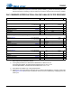
Parameter (Note 7,10) Symbol Min Typ Max Unit
Combined Digital and On-chip Analog Filter Response Single-Speed Mode
Passband (Note 7) to -0.1 dB corner
to -3 dB corner
0
0
-
-
0.35
0.4992
Fs
Fs
Frequency Response 10 Hz to 20 kHz -0.175 - +0.01 dB
StopBand 0.5465 - - Fs
StopBand Attenuation (Note 8) 50 - - dB
Group Delay tgd - 10/Fs - s
De-emphasis Error (Note 9) Fs = 44.1 kHz - - +0.05/-0.25 dB
Combined Digital and On-chip Analog Filter Response Double-Speed Mode
Passband (Note 7) to -0.1 dB corner
to -3 dB corner
0
0
-
-
0.22
0.501
Fs
Fs
Frequency Response 10 Hz to 20 kHz -0.15 - +0.15 dB
StopBand 0.5770 - - Fs
StopBand Attenuation (Note 8) 55 - - dB
Group Delay tgd - 5/Fs - s
Combined Digital and On-chip Analog Filter Response Quad-Speed Mode
Passband (Note 7) to -0.1 dB corner
to -3 dB corner
0
0
-
-
0.110
0.469
Fs
Fs
Frequency Response 10 Hz to 20 kHz -0.12 - 0 dB
StopBand 0.7 - - Fs
StopBand Attenuation (Note 8) 51 - - dB
Group Delay tgd - 2.5/Fs - s