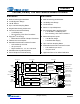
CS4245 104 dB, 24-Bit, 192 kHz Stereo Audio CODEC D/A Features A/D Features Multi-bit Delta Sigma Modulator Multi-bit Delta Sigma Modulator 104 dB Dynamic Range 104 dB Dynamic Range -90 dB THD+N -95 dB THD+N Up to 192 kHz Sampling Rates Stereo 6:1 Input Multiplexer Single-Ended Analog Architecture Volume Control with Soft Ramp Programmable Gain Amplifier (PGA) Popguard® Technology Stereo Microphone Inputs – – – – 0.
CS4245 System Features General Description Direct Interface with 1.8 V to 5 V Logic Levels The CS4245 is a h ighly integrated stereo audio CODEC. The CS4245 performs stereo analog-to-digital (A/D) and digital-to-analog (D/A) conversion of up to 24-bit serial values at sample rates up to 192 kHz.
CS4245 TABLE OF CONTENTS 1. PIN DESCRIPTIONS ........................................................................................................................ 7 2. CHARACTERISTICS AND SPECIFICATIONS ...................................................................................... 9 SPECIFIED OPERATING CONDITIONS ............................................................................................. 9 ABSOLUTE MAXIMUM RATINGS .................................................................
CS4245 6.2.4 Power-Down DAC (Bit 1) ....................................................................................................... 43 6.2.5 Power-Down Device (Bit 0) ................................................................................................... 43 6.3 DAC Control - Address 03h ............................................................................................................ 43 6.3.1 DAC Functional Mode (Bits 7:6) .......................................................
CS4245 LIST OF FIGURES Figure 1.DAC Output Test Load ................................................................................................................ 12 Figure 2.Maximum DAC Loading .............................................................................................................. 12 Figure 3.Master Mode Timing - Serial Audio Port 1 .................................................................................. 23 Figure 4.Slave Mode Timing - Serial Audio Port 1 ...............
CS4245 Table 6. Freeze-able Bits .......................................................................................................................... 42 Table 7. Functional Mode Selection ......................................................................................................... 43 Table 8. DAC Digital Interface Formats .................................................................................................... 43 Table 9. De-Emphasis Control .....................................
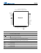
CS4245 SDIN SCLK2 LRCK2 MCLK2 SDOUT SCLK1 LRCK1 MCLK1 DGND VD INT OVFL 1.
CS4245 AGND 13 Analog Ground (Input) - Ground reference for the internal analog section. VA 14 Analog Power (Input) - Positive power for the internal analog section. AFILTA 15 Antialias Filter Connection (Output) - Antialias filter connection for the channel A ADC input. AFILTB 16 Antialias Filter Connection (Output) - Antialias filter connection for the channel B ADC input. VQ1 17 Quiescent Voltage 1 (Output) - Filter connection for the internal quiescent reference voltage.
CS4245 2. CHARACTERISTICS AND SPECIFICATIONS SPECIFIED OPERATING CONDITIONS AGND = DGND = 0 V; All voltages with respect to ground. Parameters DC Power Supplies: Symbol Min Nom Max Units VA VD VLS VLC TA 3.13 3.13 1.71 1.71 -10 5.0 3.3 3.3 3.3 - 5.25 (Note 1) 5.25 5.25 +70 V V V V C Analog Digital Logic - Serial Port Logic - Control Port Ambient Operating Temperature (Power Applied) Notes: 1. Maximum of VA+0.25 V or 5.25 V, whichever is less.
CS4245 DAC ANALOG CHARACTERISTICS Test Conditions (unless otherwise specified): AGND = DGND = 0 V; VA = 3.13 V to 5.25 V; VD = 3.13 V to 5.25 V or VA + 0.25 V, whichever is less; VLS = VLC = 1.71 V to 5.25 V; TA = -10° to +70° C for Commercial or -40° to +85° C for Automotive; Output test signal: 997 Hz full-scale sine wave; Test load RL = 3 k, CL = 10 pF (see Figure 1), Fs = 48/96/192 kHz. Measurement Bandwidth 10 Hz to 20 kHz Synchronous mode; All Connections as shown in Figure 12 on page 29.
CS4245 6. Guaranteed by design. See Figure 2. RL and CL reflect the recommended minimum resistance and maximum capacitance required for the internal op-amp’s stability. CL affects the dominant pole of the internal output amp; increasing CL beyond 100 pF can cause the internal op-amp to become unstable.
CS4245 3.3 µF V out AOUTx R L AGND C L Capacitive Load -- C L (pF) 125 100 75 25 2.5 3 Figure 1. DAC Output Test Load 12 Safe Operating Region 50 5 10 15 20 Resistive Load -- RL (k ) Figure 2.
CS4245 ADC ANALOG CHARACTERISTICS Test conditions (unless otherwise specified): AGND = DGND = 0 V; VA = 3.13 V to 5.25 V; VD = 3.13 V to 5.25 V or VA + 0.25 V, whichever is less; VLS = VLC = 1.71 V to 5.25 V; TA = -10° to +70° C for Commercial or -40° to +85° C for Automotive; Input test signal: 1 kHz sine wave; measurement bandwidth is 10 Hz to 20 kHz; Fs = 48/96/192 kHz. Synchronous mode; All connections as shown in Figure 12 on page 29. Line-Level Inputs Parameter Dynamic Performance for VA = 4.
CS4245 DC Accuracy Gain Error Gain Drift - 100 10 - % ppm/°C 0.51*VA 6.12 0.57*VA 6.8 0.63*VA 7.48 Vpp k - 5 - % Line-Level Input Characteristics Full-scale Input Voltage Input Impedance Maximum Interchannel Input Impedance Mismatch (Note 11) Line-Level and Microphone-Level Inputs Commercial Grade Parameter Symbol Min Typ Max Unit - 0.1 - dB - 0.5 - 0.4 dB dB DC Accuracy Interchannel Gain Mismatch Programmable Gain Characteristics Gain Step Size Absolute Gain Step Error 11.
CS4245 ADC ANALOG CHARACTERISTICS (Continued) Microphone-Level Inputs Parameter Dynamic Performance for VA = 4.75 V to 5.
CS4245 ADC DIGITAL FILTER CHARACTERISTICS Parameter (Notes 15, 17) Symbol Min Typ Max Unit 0 - 0.4896 Fs - - 0.035 dB 0.5688 - - Fs 70 - - dB - 12/Fs - s 0 - 0.4896 Fs - - 0.025 dB Single-Speed Mode Passband (-0.1 dB) Passband Ripple Stopband Stopband Attenuation Total Group Delay (Fs = Output Sample Rate) tgd Double-Speed Mode Passband (-0.1 dB) Passband Ripple Stopband Stopband Attenuation Total Group Delay (Fs = Output Sample Rate) tgd 0.
CS4245 AUXILIARY OUTPUT ANALOG CHARACTERISTICS Test conditions (unless otherwise specified): AGND = DGND = 0 V; VA = 3.13 V to 5.25 V; VD = 3.13 V to 5.25 V or VA + 0.25 V, whichever is less; VLS = VLC = 1.71 V to 5.25 V; TA = -10° to +70° C for Commercial or -40° to +85° C for Automotive; Input test signal: 1 kHz sine wave; Measurement bandwidth: 10 Hz to 20 kHz; Fs = 48/96/192 kHz; Synchronous mode; All connections as shown in Figure 12 on page 29. VA = 4.75 V to 5.
CS4245 AUXILIARY OUTPUT ANALOG CHARACTERISTICS (Continued) VA = 3.13 V to 3.
CS4245 20. Referred to the typical DAC Full-Scale Output Voltage. AUXILIARY OUTPUT ANALOG CHARACTERISTICS (Continued) VA = 3.13 V to 5.25 V Commercial Grade Automotive Grade Parameter Symbol Min DC Accuracy with PGA Output Selected, Line Level Input Typ Max Min Typ Max Unit Interchannel Gain Mismatch Gain Error Gain Drift - 0.1 5 100 - - 0.1 5 100 - dB % ppm/°C - 0.3 5 300 - - 0.3 5 300 - dB % ppm/°C - 100 0.1 - - 100 0.1 - dB ppm/°C -0.
CS4245 DC ELECTRICAL CHARACTERISTICS AGND = DGND = 0 V, all voltages with respect to ground. MCLK=12.288 MHz; Fs=48 kHz; Master Mode. Parameter Symbol Min Typ Max Unit V V V V IA IA ID ID - 41 37 39 23 50 45 47 28 mA mA mA mA VA = 5 V VLS, VLC, VD=5 V IA ID - 0.50 0.54 - mA mA Power Consumption (Normal Operation) VA, VD, VLS, VLC = 5 V (Power-Down Mode) VA, VD, VLS, VLC = 3.3 V VA, VD, VLS, VLC = 5 V - - 400 198 4.2 485 241 - mW mW mW PSRR - 55 - dB VQ1 - 0.
CS4245 DIGITAL INTERFACE CHARACTERISTICS Test conditions (unless otherwise specified): AGND = DGND = 0 V; VLS = VLC = 1.71 V to 5.25 V. Parameters (Note 26) High-Level Input Voltage VL = 1.71 V VL > 2.
CS4245 SWITCHING CHARACTERISTICS - SERIAL AUDIO PORT 1 Logic ‘0’ = DGND = AGND = 0 V; Logic ‘1’ = VL, CL = 20 pF. (Note 28) Parameter Sample Rate Single Speed Mode Double Speed Mode Quad Speed Mode Symbol Min Typ Max Unit Fs Fs Fs 4 50 100 - 50 100 200 kHz kHz kHz fmclk tclkhl 1.024 8 - 51.
CS4245 LRCK1 Output t slr SCLK1 Output t sdo SDOUT Figure 3. Master Mode Timing - Serial Audio Port 1 LRCK1 Input t slr t sclkh t sclkl SCLK1 Input t sdo t sclkw SDOUT Figure 4.
CS4245 SWITCHING CHARACTERISTICS - SERIAL AUDIO PORT 2 Logic ‘0’ = DGND = AGND = 0 V; Logic ‘1’ = VL, CL = 20 pF. (Note 29) Parameter Sample Rate Single Speed Mode Double Speed Mode Quad Speed Mode Symbol Min Typ Max Unit Fs Fs Fs 4 50 100 - 50 100 200 kHz kHz kHz fmclk tclkhl 1.024 8 - 51.
CS4245 LRCK2 Output t slr SCLK2 Output t sdis t sdih SDIN Figure 5. Master Mode Timing - Serial Audio Port 2 LRCK2 Input t t sclkh slr t sclkl SCLK2 Input t sclkw t sdis t sdih SDIN Figure 6.
CS4245 Channel B - Right Channel A - Left LRCK SCLK SDATA MSB -1 -2 -3 -4 -5 +5 +4 +3 +2 +1 LSB MSB -1 -2 -3 +5 -4 +4 +3 +2 +1 LSB Figure 7. Format 0, Left-Justified up to 24-Bit Data Channel A - Left LRCK Channel B - Right SCLK SDATA MSB -1 -2 -3 -4 -5 +5 +4 +3 +2 +1 LSB MSB -1 -2 -3 +5 +4 +3 +2 +1 LSB -4 Figure 8.
CS4245 SWITCHING CHARACTERISTICS - CONTROL PORT - I²C FORMAT Inputs: Logic 0 = DGND = AGND = 0 V, Logic 1 = VLC, CL = 30 pF. Parameter Symbol Min Max Unit SCL Clock Frequency fscl - 100 kHz RESET Rising Edge to Start tirs 500 - ns Bus Free Time Between Transmissions tbuf 4.7 - µs Start Condition Hold Time (prior to first clock pulse) thdst 4.0 - µs Clock Low time tlow 4.7 - µs Clock High Time thigh 4.0 - µs tsust 4.
CS4245 SWITCHING CHARACTERISTICS - CONTROL PORT - SPI FORMAT Inputs: Logic 0 = DGND = AGND = 0 V, Logic 1 = VLC, CL = 30 pF. Parameter Symbol Min Max Units CCLK Clock Frequency fsck - 6.0 MHz RESET Rising Edge to CS Falling tsrs 500 - ns CS High Time Between Transmissions tcsh 1.
CS4245 3. TYPICAL CONNECTION DIAGRAM +3.3V to +5V 10 µF VD +1.8V to +5V 0.1 µF 3.3 µF AUXOUTA VLS 3.3 µF AUXOUTB MCLK2 Mute Drive MUTEC LRCK2 3.3 µF SDIN AOUTA SCLK1 AOUTB LRCK1 INT AIN1A CS4245 OVFL AIN1B RESET MicroController AIN2A SCL/CCLK SDA/CDOUT AD1/CDIN AIN2B AD0/CS 2 k AIN3A 2 k See Note 1 +1.8V to +5V VLC AIN3B 0.
CS4245 4. APPLICATIONS 4.1 Recommended Power-Up Sequence 1. Hold RESET low until the power supply, MCLK1, MCLK2 (if used), LRCK1 and LRCK2 are stable. In this state, the Control Port is reset to its default settings. 2. Bring RESET high. The device will remain in a low power state with the PDN bit set by default. The control port will be accessible. 3. The desired register settings can be loaded while the PDN bit remains set. 4. Clear the PDN bit to initiate the power-up sequence. 4.
CS4245 in Master Mode, and receive the proper clocks in Slave Mode. Table 2 illustrates several standard audio sample rates and the required MCLK and LRCK frequencies. LRCK (kHz) MCLK (MHz) 64x 96x 128x 192x 256x 384x 512x 768x 1024x 32 - - - - 8.1920 12.2880 16.3840 24.5760 32.7680 44.1 - - - - 11.2896 16.9344 22.5792 33.8680 45.1584 48 - - - - 12.2880 18.4320 24.5760 36.8640 49.1520 64 - - 8.1920 12.2880 16.3840 24.5760 32.7680 - - 88.2 - - 11.2896 16.
CS4245 4.2.3 Master Mode As a clock master, LRCK and SCLK will operate as outputs. The two serial ports may be independently placed into Master or Slave mode. Each LRCK and SCLK is internally derived from its respective MCLK with LRCK equal to Fs and SCLK equal to 64 x Fs as shown in Figure 13. MCLK1 Freq Bits MCLK1 ÷1 000 ÷1.5 001 ÷2 010 ÷3 011 ÷4 100 MCLK2 Freq Bits MCLK2 00 ÷128 01 ÷64 10 000 ÷1.
CS4245 The high-pass filter continuously subtracts a measure of the DC offset from the output of the decimation filter. If the HPFFreeze bit (See “ADC High-Pass Filter Freeze (Bit 1)” on page 45.) is set during normal operation, the current value of the DC offset for the each channel is frozen and this DC offset will continue to be subtracted from the conversion result. This feature makes it possible to perform a system DC offset calibration by: 1.
CS4245 4.4 Analog Input Multiplexer, PGA, and Mic Gain The CS4245 contains a stereo 6-to-1 analog input multiplexer followed by a programmable gain amplifier (PGA). The input multiplexer can select one of six possible stereo analog input sources and route it to the PGA. Analog inputs 4A and 4B are able to insert a +32 dB gain stage before the input multiplexer, allowing them to be used for microphone-level signals without the need for any external gain.
CS4245 4.7 Output Transient Control The CS4245 uses Popguard® technology to minimize the effects of output transients during power-up and power-down. This technique eliminates the audio transients commonly produced by single-ended, singlesupply converters when it is implemented with external DC-blocking capacitors connected in series with the audio outputs. To make best use of this feature, it is necessary to understand its operation. 4.7.
CS4245 De-emphasis is only available in Single-Speed Mode. Gain dB T1=50 µs 0dB T2 = 15 µs -10dB F1 3.183 kHz F2 Frequency 10.61 kHz Figure 15. De-Emphasis Curve 4.10 Internal Digital Loopback The CS4245 supports an internal digital loopback mode in which the output of the ADC is routed to the input of the DAC. This mode may be activated by setting the LOOP bit in the Signal Selection register (See Section 6.6 “Signal Selection - Address 06h” on page 46).
CS4245 signer to achieve idle channel noise/signal-to-noise ratios which are only limited by the external mute circuit. The MUTEC pin is an active-low CMOS driver. See Figure 16 for a suggested active-low mute circuit. +VEE AC Couple AOUT 560 LPF Audio Out 47 k CS4245 -VEE +VA MMUN2111LT1 MUTEC 2 k 10 k -VEE Figure 16. Suggested Active-Low Mute Circuit 4.
CS4245 dress and set the read/write bit (R/W) high. The next falling edge of CCLK will clock out the MSB of the addressed register (CDOUT will leave the high-impedance state). For both read and write cycles, the memory address pointer will automatically increment following each data byte in order to facilitate block reads and writes of successive registers.
CS4245 0 1 2 3 4 5 6 7 8 9 10 11 12 13 14 15 16 17 18 19 20 21 22 23 24 25 26 27 28 SCL CHIP ADDRESS (WRITE) SDA 1 0 0 1 STOP MAP BYTE 7 1 AD1 AD0 0 6 5 4 3 ACK 2 1 CHIP ADDRESS (READ) 1 0 0 0 1 ACK START DATA 1 AD1 AD0 1 START 7 ACK DATA +1 0 7 ACK 0 DATA + n 7 0 NO ACK STOP Figure 19. Control Port Timing, I²C Read Since the read operation cannot set the MAP, an aborted write operation is used as a preamble.
CS4245 4.14 Reset When RESET is low, the CS4245 enters a low-power mode and all internal states are reset, including the control port and registers, the outputs are muted. When RESET is high, the control port becomes operational, and the desired settings should be loaded into the control registers. Writing a 0 to the PDN bit in the Power Control register will then cause the part to leave the low-power state and begin operation.
CS4245 5. REGISTER QUICK REFERENCE This table shows the register names and their associated default values.
CS4245 6. REGISTER DESCRIPTION 6.1 Chip ID - Register 01h 7 PART3 6 PART2 5 PART1 4 PART0 3 REV3 2 REV2 1 REV1 0 REV0 Function: This register is Read-Only. Bits 7 through 4 are the part number ID, which is 1100b (0Ch), and the remaining bits (3 through 0) indicate the device revision as shown in Table 5 below. REV[2:0] Revision 001 A 010 B, C0 011 C1 Table 5. Device Revision 6.2 Power Control - Address 02h 7 Freeze 6.2.
CS4245 6.2.4 Power-Down DAC (Bit 1) Function: The DAC pair will remain in a reset state whenever this bit is set. 6.2.5 Power-Down Device (Bit 0) Function: The device will enter a low-power state whenever this bit is set. The power-down bit is set by default and must be cleared before normal operation can occur. The contents of the control registers are retained when the device is in power-down. 6.
CS4245 6.3.4 De-Emphasis Control (Bit 1) Function: The standard 50/15 s digital de-emphasis filter response, Figure 20, may be implemented for a sample rate of 44.1 kHz when the DeEmph bit is configured as shown in Table 9. NOTE: De-emphasis is available only in Single-Speed Mode. DeEmph 0 1 Description Disabled (default) 44.1 kHz de-emphasis Table 9. De-Emphasis Control Gain dB T1=50 µs 0dB T2 = 15 µs -10dB F1 3.183 kHz F2 Frequency 10.61 kHz Figure 20. De-Emphasis Curve 6.3.
CS4245 6.4.2 ADC Digital Interface Format (Bit 4) Function: The required relationship between LRCK1, SCLK1 and SDOUT is defined by the ADC Digital Interface Format bit. The options are detailed in Table 11 and may be seen in Figure 7 and Figure 8. ADC_DIF Description Format Figure 0 Left-Justified, up to 24-bit data (default) 0 7 1 I²S, up to 24-bit data 1 8 Table 11. ADC Digital Interface Formats 6.4.
CS4245 6.5.2 Master Clock 2 Frequency (Bits 2:0) Function: These bits set the frequency of the supplied MCLK2 signal. See Table 13 for the appropriate settings. MCLK2 Divider MCLK2 Freq2 MCLK2 Freq1 MCLK2 Freq0 ÷1 0 0 0 ÷ 1.5 0 0 1 ÷2 0 1 0 ÷3 0 1 1 ÷4 1 0 0 Reserved 1 0 1 Reserved 1 1 x Table 13. MCLK 2 Frequency 6.6 Signal Selection - Address 06h 7 6 5 4 3 2 1 0 Reserved AOutSel1 AOutSel0 Reserved Reserved Reserved LOOP ASynch 6.6.
CS4245 6.7 Channel B PGA Control - Address 07h 7 Reserved 6.7.1 6 Reserved 5 Gain5 4 Gain4 3 Gain3 2 Gain2 1 Gain1 0 Gain0 3 Gain3 2 Gain2 1 Gain1 0 Gain0 Channel B PGA Gain (Bits 5:0) Function: See “Channel A PGA Gain (Bits 5:0)” on page 47. 6.8 Channel A PGA Control - Address 08h 7 Reserved 6.8.1 6 Reserved 5 Gain5 4 Gain4 Channel A PGA Gain (Bits 5:0) Function: Sets the gain or attenuation for the ADC input PGA stage. The gain may be adjusted from -12 dB to +12 dB in 0.5 dB steps.
CS4245 occur after a time-out period between 512 and 1024 sample periods (10.7 ms to 21.3 ms at 48 kHz sample rate) if the signal does not encounter a zero crossing. The zero cross function is independently monitored and implemented for each channel. See Table 16. PGASoft 0 0 1 1 PGAZeroCross 0 1 0 1 Mode Changes to affect immediately Zero Cross enabled Soft Ramp enabled Soft Ramp and Zero Cross enabled (default) Table 16. PGA Soft Cross or Zero Cross Mode Selection 6.9.
CS4245 shown in Table 18. The volume changes are implemented as dictated by the DACSoft and DACZeroCross bits in the DAC Control 2 register (see Section 6.12.1). Binary Code Volume Setting 00000000 0 dB 00000001 -0.5 dB 00101000 -20 dB 00101001 -20.5 dB 11111110 -127 dB 11111111 -127.5 dB Table 18. Digital Volume Control Example Settings 6.12 DAC Control 2 - Address 0Ch 7 6 5 4 3 2 1 0 DACSoft DACZero InvertDAC Reserved Reserved Reserved Reserved Active_H/L 6.12.
CS4245 6.12.3 Active High/Low (Bit 0) Function: When this bit is set, the INT pin functions as an active high CMOS driver. When this bit is cleared, the INT pin functions as an active low open drain driver and will require an external pull-up resistor for proper operation. 6.
CS4245 6.15 Interrupt Mode MSB - Address 0Fh 6.16 Interrupt Mode LSB - Address 10h 7 Reserved Reserved 6 Reserved Reserved 5 Reserved Reserved 4 Reserved Reserved 3 ADCClkErr1 ADCClkErr0 2 DACClkErr1 DACClkErr0 1 ADCOvfl1 ADCOvfl0 0 ADCUndrfl1 ADCUndrfl0 Function: The two Interrupt Mode registers form a 2-bit code for each Interrupt Status register function. There are three ways to set the INT pin active in accordance with the interrupt condition.
CS4245 7. PARAMETER DEFINITIONS Dynamic Range The ratio of the rms value of the signal to the rms sum of all other spectral components over the specified bandwidth. Dynamic Range is a signal-to-noise ratio measurement over the specified bandwidth made with a -60 dBFS signal. 60 dB is added to resulting measurement to refer the measurement to full scale. This technique ensures that the distortion components are below the noise level and do not affect the measurement.
CS4245 8. DAC FILTER PLOTS Figure 21. DAC Single-Speed Stopband Rejection Figure 22. DAC Single-Speed Transition Band 0 -1 0.05 -2 0 -3 -0.05 Amplitude dB Amplitude dB -4 -5 -6 -0. 1 -0.15 -7 -0. 2 -8 -0.25 -9 -10 0.45 0.46 0.47 0.48 0.49 0.5 0.51 Frequency (normalized to Fs) 0.52 0.53 0.54 0.5 5 0 0.05 0.1 0.15 0.2 0.25 0.3 Frequency (normalized to Fs) 0.35 0.4 0.45 Figure 23. DAC Single-Speed Transition Band Figure 24. DAC Single-Speed Passband Ripple Figure 25.
CS4245 1 0.8 0 0.7 -1 0.6 -2 0.5 Amplitude dB Amplitude dB -3 -4 -5 0.4 0.3 0.2 -6 0.1 -7 0 -8 -0. 1 -9 - 10 0.45 0.46 0.47 0.48 0.49 0.5 0.51 Frequency (normalized to Fs) 0.52 0.53 0.54 -0. 2 0.55 0 Figure 27. DAC Double-Speed Transition Band 0.05 0.1 0.15 0.2 0.25 0.3 Frequency (normalized to Fs) 0.35 0.4 0.45 0.5 Figure 28.
CS4245 0 -10 -20 -30 -40 -50 -60 -70 -80 -90 -100 -110 -120 -130 -140 Amplitude (dB) Amplitude (dB) 9. ADC FILTER PLOTS 0.0 0.1 0.2 0.3 0.4 0.5 0.6 0.7 0.8 0.9 1.0 0 -10 -20 -30 -40 -50 -60 -70 -80 -90 -100 -110 -120 -130 -140 0.40 0.42 0.44 Frequency (norm alized to Fs) 0 0.10 -1 0.08 -2 0.06 -3 0.04 -4 -5 -6 -7 0.58 0.60 0.00 -0.04 -0.06 -0.08 -0.10 0.46 0.47 0.48 0.49 0.5 0.51 0.52 0.53 0.54 0 0.55 Figure 35.
0 0.10 -1 0.08 -2 0.06 -3 0.04 Amplitude (dB) Amplitude (dB) CS4245 -4 -5 -6 -7 0.02 0.00 -0.02 -0.04 -8 -0.06 -9 -0.08 -10 0.46 0.47 0.48 0.49 0.50 0.51 -0.10 0.00 0.05 0.52 Frequency (norm alized to Fs) 0 -10 -20 -30 -40 -50 -60 -70 -80 -90 -100 -110 -120 -130 -140 0.1 0.2 0.3 0.4 0.5 0.6 0.7 0.8 0.15 0.20 0.25 0.30 0.35 0.40 0.45 0.50 Figure 40. ADC Double-Speed Passband Ripple Amplitude (dB) Amplitude (dB) Figure 39. ADC Double-Speed Transition Band (Detail) 0.
CS4245 10.PACKAGE DIMENSIONS 48L LQFP PACKAGE DRAWING E E1 D D1 1 e B A A1 L DIM A A1 B D D1 E E1 e* L MIN --0.002 0.007 0.343 0.272 0.343 0.272 0.016 0.018 0.000° * Nominal pin pitch is 0.50 mm INCHES NOM MAX MIN 0.055 0.063 --0.004 0.006 0.05 0.009 0.011 0.17 0.354 0.366 8.70 0.28 0.280 6.90 0.354 0.366 8.70 0.28 0.280 6.90 0.020 0.024 0.40 0.24 0.030 0.45 4° 7.000° 0.00° *Controlling dimension is mm. MILLIMETERS NOM MAX 1.40 1.60 0.10 0.15 0.22 0.27 9.0 BSC 9.30 7.0 BSC 7.10 9.0 BSC 9.30 7.
CS4245 12.ORDERING INFORMATION Product CS4245 CS4245 CDB4245 Description 24-bit, 192 kHz Stereo Audio CODEC 24-bit, 192 kHz Stereo Audio CODEC Package Pb-Free 48-LQFP 48-LQFP CS4245 Evaluation Board Yes Grade Commercial Temp Range -10° to +70° C Yes Automotive -40° to +105° C No - - Container Order # Tray CS4245-CQZ Tape & Reel CS4245-CQZR Tray CS4245-DQZ Tape & Reel CS4245-DQZR - CDB4245 13.
CS4245 Contacting Cirrus Logic Support For all product questions and inquiries, contact a Cirrus Logic Sales Representative. To find the one nearest you, go to www.cirrus.com IMPORTANT NOTICE Cirrus Logic, Inc. and its subsidiaries (“Cirrus”) believe that the information contained in this document is accurate and reliable. However, the information is subject to change without notice and is provided “AS IS” without warranty of any kind (express or implied).