
User guide

DS900F1 6
CS4244
1.1 I/O Pin Characteristics
Input and output levels and associated power supply voltage are shown in the table below. Logic levels
should not exceed the corresponding power supply voltage.
Notes:
1. Internal connection valid when device is in reset.
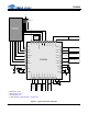
2. This pin has no internal pull-up or pull-down resistors. External pull-up or pull-down resistors should
be added in accordance with Figure 2.
VA 20 Analog Power (Input) - Positive power for the analog sections.
VQ 22 Quiescent Voltage (Output) - Filter connection for internal quiescent voltage.
VREF 23 Analog Power Reference (Input) - Return pin for the VBIAS cap.
VBIAS 24 Positive Voltage Reference (Output) - Positive reference voltage for the internal DACs.
AOUTx-
25,27,29,
31
Negative Analog Output (Output) - Negative output signals from the internal digital to analog con-
verters. The full scale analog output level is specified in the
Analog Output Characteristics tables
on pages 15 and 16
.
AOUTx+
26,28,30,
32
Positive Analog Output (Output) - Positive output signals from the internal digital to analog convert-
ers. The full scale analog output level is specified in the Analog Output Characteristics tables on
pages 15 and 16
.
TSTOx 33,34 Test Outputs (Output) - Test outputs. These pins should be left unconnected.
RST
35 Reset (Input) - Applies reset to the internal circuitry when pulled low.
INT
36 Interrupt (Output) - Sent to DSP to indicate an interrupt condition has occurred.
AD2/SDOUT2 37
I²C Address Bit 2/Serial Data Output 2 (Input/Output) - Sets the I²C address bit 2 at reset. Func-
tions as Serial Data Out 2 for AIN3 and AIN4 ADC data output in Left Justified and I²S modes. High
impedance in TDM mode. See Section 4.3 I²C Control Port for more details concerning this mode of
operation.
AD1 38 I²C Address Bit 1 (Input) - Sets the I²C address bit 1.
AD0 39 I²C Address Bit 0 (Input) - Sets the I²C address bit 0.
SCL 40 Serial Control Port Clock (Input) - Serial clock for the I²C control port.
GND -
Thermal Pad - The thermal pad on the bottom of the device should be connected to the ground
plane via an array of vias.
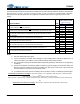
Power Supply Pin Name I/O Driver
Internal Connections
(Note 1)
Receiver
VL
SCL Input - Weak Pull-down (~500k 5.0 V CMOS, with Hysteresis
SDA Input/Output
CMOS/Open
Drain
Weak Pull-down (~500k 5.0 V CMOS, with Hysteresis
I
NT Output
CMOS/Open
Drain
(Note 2) -
RST
Input - (Note 2) 5.0 V CMOS, with Hysteresis
MCLK Input - Weak Pull-down (~500k 5.0 V CMOS, with Hysteresis
FS/LRCK Input/Output 5.0 V CMOS Weak Pull-down (~500k 5.0 V CMOS, with Hysteresis
SCLK Input/Output 5.0 V CMOS Weak Pull-down (~500k 5.0 V CMOS, with Hysteresis
SDOUT1 Output 5.0 V CMOS Weak Pull-down (~500k
SDINx Input - Weak Pull-down (~500k 5.0 V CMOS, with Hysteresis
AD0,1 Input - (Note 2) 5.0 V CMOS
AD2/SDOUT2 Input/Output 5.0 V CMOS (Note 2) 5.0 V CMOS