
User guide

DS900F1 19
CS4244
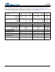
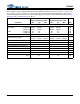
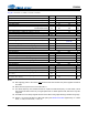
SWITCHING CHARACTERISTICS - SERIAL AUDIO INTERFACE
VA_SEL = 0 for VA = 3.3 VDC, 1 for VA = 5.0 VDC.
Notes:
25. After applying power to the
CS4244, RST should be held low until after the power supplies and MCLK
are stable.
26. MCLK must be synchronous to and scale with F
S
.
27. The SCLK frequency must remain less than or equal to the MCLK frequency. For this reason, SCLK
may range from 256x to 512x only in single speed mode. In double speed mode, 256x is the only ratio
supported.
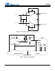
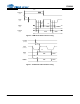
28. The MSB of CH1 is always aligned with the second SCLK rising edge following FS/LRCK rising edge.
29. Where “n” is equal to the MCLK to LRCK ratio (set by the Master Clock Rate register bits), i.e. in 256x
mode, n = 256, in 512x mode, n = 512, etc.
Parameters Symbol Min Max Units
RST pin Low Pulse Width (Note 25) 1
-ms
MCLK Frequency
(Note 26) 7.68 25.6 MHz
MCLK Duty Cycle 45 55 %
SCLK Duty Cycle 45 55 %
Input Sample Rate (FS/LRCK pin) Single-Speed Mode
Double-Speed Mode
F
S
F
S
30
60
50
100
kHz
kHz
SCLK Falling Edge to SDOUTx Valid (VL = 1.8 V) t
dh2
-31ns
SCLK Falling Edge to SDOUTx Valid (VL = 2.5 V) t
dh2
-22ns
SCLK Falling Edge to SDOUTx Valid (VL = 3.3 V or 5 V) t
dh2
-17ns
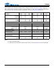
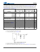
TDM Slave Mode
SCLK Frequency
(Note 27) 256x 512x F
S
FS/LRCK High Time Pulse (Note 28)
t
lpw
1/f
SCLK
(n-1)/f
SCLK
(Note 29)
ns
FS/LRCK Rising Edge to SCLK Rising Edge t
lcks
5-ns
SDINx Setup Time Before SCLK Rising Edge t
ds
3-ns
SDINx Hold Time After SCLK Rising Edge t
dh1
5-ns
PCM Slave Mode
SCLK Frequency 32x 64x F
S
FS/LRCK Duty Cycle 45 55 %
FS/LRCK Edge to SCLK Rising Edge t
lcks
5-ns
SDINx Setup Time Before SCLK Rising Edge t
ds
3-ns
SDINx Hold Time After SCLK Rising Edge t
dh1
5-ns
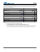
PCM Master Mode
SCLK Frequency 64x 64x F
S
FS/LRCK Duty Cycle 45 55 %
FS/LRCK Edge to SCLK Rising Edge t
lcks
5-ns
SDINx Setup Time Before SCLK Rising Edge t
ds
5-ns
SDINx Hold Time After SCLK Rising Edge
(VL=1.8V)
t
dh1
11 - ns
SDINx Hold Time After SCLK Rising Edge
(VL=2.5V, 3.3V, or 5V)
t
dh1
10 - ns