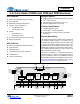
CS4244 4 In/4 Out Audio CODEC with PCM and TDM Interfaces DAC Features System Features Advanced multibit delta-sigma modulator 24-bit resolution Differential or single-ended outputs Dynamic range (A-weighted) – -109 dB differential – Common Applications Automotive audio systems AV, Blu-Ray®, and DVD receivers Audio interfaces, mixing consoles, and effects processors -105 dB single-ended THD+N – -90 dB differential – -88 dB single ended General Description 2 Vrms full-scal
CS4244 TABLE OF CONTENTS 1. PIN DESCRIPTIONS ............................................................................................................................ 5 1.1 I/O Pin Characteristics ..................................................................................................................... 6 2. TYPICAL CONNECTION DIAGRAM ................................................................................................... 7 3. CHARACTERISTICS AND SPECIFICATIONS ......................
CS4244 LIST OF FIGURES Figure 1. CS4244 Pinout ............................................................................................................................. 5 Figure 2. Typical Connection Diagram ........................................................................................................ 7 Figure 3. Test Circuit for ADC Performance Testing ................................................................................. 13 Figure 4. PSRR Test Configuration .......................
CS4244 LIST OF TABLES Table 1. Speed Modes .............................................................................................................................. 26 Table 2. Common Clock Frequencies ....................................................................................................... 26 Table 3. Master Mode Left Justified and I²S Clock Ratios ........................................................................ 27 Table 4. Slave Mode Left Justified and I²S Clock Ratios .........
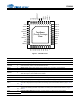
CS4244 SCL AD0 AD1 AD2/SDOUT2 INT RST TSTO1 TSTO2 AOUT1+ AOUT1- 40 39 38 37 36 35 34 33 32 31 1. PIN DESCRIPTIONS SDA 1 30 AOUT2+ SDIN1 2 29 AOUT2- SDIN2 3 28 AOUT3+ FS/LRCK 4 27 AOUT3- MCLK 5 26 AOUT4+ SCLK 6 25 AOUT4- SDOUT1 7 24 VBIAS VL 8 23 VREF GND 9 22 VQ VDREG 10 21 GND 19 20 FILT+ VA 16 AIN2- 18 15 AIN3- AIN2+ AIN1- 14 AIN3+ 17 13 AIN4- AIN1+ 12 AIN4+ 11 Top-Down (Though Package) View Figure 1.
CS4244 VA 20 Analog Power (Input) - Positive power for the analog sections. VQ 22 Quiescent Voltage (Output) - Filter connection for internal quiescent voltage. VREF 23 Analog Power Reference (Input) - Return pin for the VBIAS cap. VBIAS 24 Positive Voltage Reference (Output) - Positive reference voltage for the internal DACs. AOUTx- Negative Analog Output (Output) - Negative output signals from the internal digital to analog con25,27,29, verters.
CS4244 2.
CS4244 3. CHARACTERISTICS AND SPECIFICATIONS RECOMMENDED OPERATING CONDITIONS GND = 0 V; all voltages with respect to ground. (Note 3) Parameters Symbol Min Typ Max Units Analog Core VA 3.135 4.75 3.3 5 3.465 5.25 V V Level Translator VL 1.71 - 5.25 V TA -40 0 - +85 +70 C C TJ -40 - +150 C DC Power Supply Temperature Ambient Operating Temperature - Power Applied Automotive Commercial Junction Temperature Notes: 3.
CS4244 DC ELECTRICAL CHARACTERISTICS GND = 0 V; all voltages with respect to ground. Parameters Min Typ Max Units - 2.5 0.5 - V - VA 23 - 1 V k A - 0.5•VA 77 - 0 V k A VDREG (Note 7) Nominal Voltage Output Impedance FILT+ Nominal Voltage Output Impedance DC Current Source/Sink VQ Nominal Voltage Output Impedance DC Current Source/Sink Notes: 7. No external loads should be connected to the VDREG pin.
CS4244 TYPICAL CURRENT CONSUMPTION This table represents the power consumption for individual circuit blocks within the CS4244. CS4244 is configured as shown in Figure 2 on page 7. VA_SEL = 0 for VA = 3.3 VDC, 1 for VA = 5.0 VDC; FS = 100 kHz; MCLK = 25.6 MHz; DAC load is 3 k; All input signals are zero (digital zero for SDINx inputs and AC coupled to ground for AINx inputs) .
CS4244 ANALOG INPUT CHARACTERISTICS (COMMERCIAL GRADE) Test Conditions (unless otherwise specified): Device configured as shown in Section 2. on page 7. Input sine wave: 1 kHz; VA_SEL = 0 for VA = 3.3 VDC, 1 for VA = 5.0 VDC.; TA = 25 C; Measurement Bandwidth is 20 Hz to 20 kHz unless otherwise specified; Sample Rate = 48 kHz; all Power Down ADCx bits = 0. VA, VREF = 3.3 V Parameter Min VA, VREF = 5.
CS4244 ANALOG INPUT CHARACTERISTICS (AUTOMOTIVE GRADE) Test Conditions (unless otherwise specified): Device configured as shown in Section 2. on page 7. Input sine wave: 1 kHz; VA_SEL = 0 for VA = 3.3 VDC, 1 for VA = 5.0 VDC.; TA = -40 to +85 C; Measurement Bandwidth is 20 Hz to 20 kHz unless otherwise specified; Sample Rate = 48 kHz; all Power Down ADCx bits = 0. VA, VREF = 3.3 V Parameter Min VA, VREF = 5.
CS4244 634 470 pF VA 4.7 uF - 90.9 CS4244 AINx + 100 k Analog Signal + 100 k 100 k + 2700 pF 100 k 100 k + Analog Signal 100 k 4.7 uF CS4244 AINx 90.9 - VA 470 pF 634 Figure 3. Test Circuit for ADC Performance Testing +Vcc +Vcc Operational Amplifier Power DAC DUT PWR + OUT GND GND -Vcc Analog Out - + - + OUT Analog Generator Digital Out - + Analyzer Test Equipment Figure 4.
CS4244 ADC DIGITAL FILTER CHARACTERISTICS Test Conditions (unless otherwise specified): Device configured as shown in Section 2. on page 7. Input sine wave: 1 kHz; VA_SEL = 0 for VA = 3.3 VDC, 1 for VA = 5.0 VDC.; Measurement Bandwidth is 20 Hz to 20 kHz unless otherwise specified. See filter plots in Section 7. on page 59. Parameter (Note 15) Passband (Frequency Response) Min to -0.1 dB corner Typ Max Unit 0 - 0.4535 Fs -0.09 - 0.17 dB Stopband 0.
CS4244 ANALOG OUTPUT CHARACTERISTICS (COMMERCIAL GRADE) Test Conditions (unless otherwise specified). Device configured as shown in Section 2. on page 7. VA_SEL = 0 for VA = 3.3 VDC, 1 for VA = 5.0 VDC.; TA = 25 C; Full-scale 1 kHz input sine wave; Sample Rate = 48 kHz; Measurement Bandwidth is 20 Hz to 20 kHz; Specifications apply to all channels unless otherwise indicated; all Power Down DACx bits = 0. See (Note 19) on page 16. VA, VREF= 3.3 V (Differential/Single-ended) Parameter VA, VREF= 5.
CS4244 ANALOG OUTPUT CHARACTERISTICS (AUTOMOTIVE GRADE) Test Conditions (unless otherwise specified): Device configured as shown in Section 2. on page 7. VA_SEL = 0 for VA = 3.3 VDC, 1 for VA = 5.0 VDC.; TA = -40 to +85 C; Full-scale 1 kHz input sine wave; Sample Rate = 48 kHz; Measurement Bandwidth is 20 Hz to 20 kHz; Specifications apply to all channels unless otherwise indicated; all Power Down DACx bits = 0. See (Note 19). VA, VREF= 3.3 V (Differential/Single-ended) Parameter VA, VREF= 5.
CS4244 COMBINED DAC INTERPOLATION & ON-CHIP ANALOG FILTER RESPONSE Test Conditions (unless otherwise specified): VA_SEL = 0 for VA = 3.3 VDC, 1 for VA = 5.0 VDC. The filter characteristics have been normalized to the sample rate (FS) and can be referenced to the desired sample rate by multiplying the given characteristic by FS.
CS4244 DIGITAL I/O CHARACTERISTICS Parameters High-Level Input Voltage (all input pins except RST) (% of VL) (VL = 1.8 V) High-Level Input Voltage (all input pins except RST) (% of VL) (VL = 2.5 V, 3.3 V, or 5 V) Low-Level Input Voltage (all input pins except RST) (% of VL) High-Level Input Voltage (RST pin) Low-Level Input Voltage (RST pin) Symbol Min Typ Max Units VIH 75% - - V VIH 70% - - V VIL - - 30% V VIH 1.2 - - V VIL - - 0.
CS4244 SWITCHING CHARACTERISTICS - SERIAL AUDIO INTERFACE VA_SEL = 0 for VA = 3.3 VDC, 1 for VA = 5.0 VDC. Parameters RST pin Low Pulse Width (Note 25) MCLK Frequency MCLK Duty Cycle SCLK Duty Cycle Input Sample Rate (FS/LRCK pin) (Note 26) Single-Speed Mode Double-Speed Mode SCLK Falling Edge to SDOUTx Valid (VL = 1.8 V) SCLK Falling Edge to SDOUTx Valid (VL = 2.5 V) SCLK Falling Edge to SDOUTx Valid (VL = 3.
CS4244 ~ ~ ~ tLPW FS/LRCK (input) tlcks SCLK (input) tds tdh1 SDINx MSB (input) tdh2 MSB-1 tdh2 SDOUT1 MSB (output) MSB-1 Figure 6. TDM Serial Audio Interface Timing FS/LRCK (input/output) tlcks SCLK (input/output) tds SDINx (input) tdh1 MSB MSB-1 MSB MSB-1 tdh2 SDOUTx (output) Figure 7.
CS4244 SWITCHING SPECIFICATIONS - CONTROL PORT Test conditions (unless otherwise specified): Inputs: Logic 0 = GND = 0 V, Logic 1 = VL; SDA load capacitance equal to maximum value of Cb specified below (Note 30). Parameters Symbol Min Max Unit SCL Clock Frequency fscl - 550 kHz RESET Rising Edge to Start tirs (Note 31) - ns Bus Free Time Between Transmissions tbuf 1.3 - µs Start Condition Hold Time (prior to first clock pulse) thdst 0.6 - µs Clock Low time tlow 1.
CS4244 4. APPLICATIONS 4.1 Power Supply Decoupling, Grounding, and PCB Layout As with any high-resolution converter, the CS4244 requires careful attention to power supply and grounding arrangements if its potential performance is to be realized. Figure 2 shows the recommended power arrangements, with VA connected to clean supplies. VDREG, which powers the digital circuitry, is generated internally from an on-chip regulator from the VA supply.
CS4244 4.2.2 Power-down To prevent audio transients at power-down, the DC-blocking capacitors must fully discharge before turning off the power. In order to do this in a controlled manner, it is recommended that all the converters be muted to start the sequence. Next, set PDNx for all converters to 1 to power them down internally. Then, FS/LRCK and SCLK can be removed if desired.
CS4244 and 16, the VQ voltage will never rise to its minimum operating voltage. If the VQ voltage never rises above this minimum operating voltage, the device will not finish the power-up sequence and normal operation will not begin. Also note that any AOUTx± pin(s) with a DC load must remain powered up (PDN DACx = 0) to keep the VQ net at its nominal voltage during normal operation, otherwise clipping may occur on the outputs. Note that the load capacitors (CLx) are also in parallel during power-up.
CS4244 The signal timings for a read and write cycle are shown in Figure 11 and Figure 12. A Start condition is defined as a falling transition of SDA while the clock is high. A Stop condition is a rising transition while the clock is high. All other transitions of SDA occur while the clock is low. The first byte sent to the CS4244 after a Start condition consists of a 7-bit chip address field and a R/W bit (high for a read, low for a write). The upper 4 bits of the 7-bit address field are fixed at 0010.
CS4244 4.3.1 Memory Address Pointer (MAP) The MAP byte comes after the address byte and selects the register to be read or written. Refer to the pseudocode above for implementation details. 4.3.1.1 Map Increment (INCR) The CS4244 has MAP auto-increment capability enabled by the INCR bit (the MSB) of the MAP. If INCR is set to ‘0’, MAP will stay constant for successive I²C reads or writes.
CS4244 4.4.2 Master Mode Clock Ratios As a clock master, FS/LRCK and SCLK will operate as outputs internally derived from MCLK. FS/LRCK is equal to FS and SCLK is equal to 64x FS as shown in Figure 13. TDM format is not supported in Master Mode. MCLK Rate Bits ÷512 00 01 FS/LRCK MCLK ÷1.5 x2 000 ÷256 x2 001 Speed Mode Bits ÷1 010 ÷8 00 ÷4 01 SCLK PLL active Figure 13. Master Mode Clocking The resulting valid master mode clock ratios are shown in Table 3 below.
CS4244 4.5 Serial Port Interface The serial port interface format is selected by the Serial Port Format register bits. The TDM format is available in Slave Mode only. 4.5.1 TDM Mode The serial port of the CS4244 supports the TDM interface format with varying bit depths from 16 to 24 as shown in Figure 15. Data is clocked out of the ADC on the falling edge of SCLK and clocked into the DAC on the rising edge.
DS900F1 0's [7:0] ADC1 Data[31:8] ADC1 Data[31:8] SDIN2 SDOUT1 SDOUT1 with Sidechain x [7:0] 0's [7:0] Input Data 2.1 [31:8] ADC1 Data [31:8] ADC1 Data [31:8] SDIN1 SDIN2 SDOUT1 SDOUT1 with Sidechain 0's [7:0] x [7:0] Input Data 1.1 [31:8] Slot 1 [31:0] x [7:0] Input Data 2.1 [31:8] SDIN1 0's [7:0] x [7:0] Slot 1 [31:0] Input Data 1.1 [31:8] 0's [7:0] ADC2 Data [31:8] 0's [7:0] 0's [7:0] ADC4 Data [31:8] ADC4 Data [31:8] x [7:0] Input Data 2.
CS4244 4.5.2 Left Justified and I²S Modes The serial port of the CS4244 supports the Left Justified and I²S interface formats with valid bit depths of 16, 18, 20, or 24 bits for the SDOUTx pins and 24 bits for the SDINx pins. All data is valid on the rising edge of SCLK. Data is clocked out of the ADC on the falling edge of SCLK and clocked into the DAC on the rising edge. In Master Mode each slot is 32 bits wide.
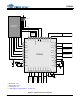
CS4244 4.6 Internal Signal Path VD 2.5 VDC 2.5 V AIN1 AIN2 AIN3 AIN4 (±) (±) (±) (±) VA 5.0 VDC LDO Analog Supply Multi-bit ADC Digital Filters Channel Volume , Mute, Invert , Noise Gate Master Volume Control Interpolation Filter Multi-bit Modulators Serial Audio Interface DAC & Analog Filters AOUT1 (±) AOUT2 (±) AOUT3 (±) AOUT4 (±) Control Port Level Translator SDOUT1 SDOUT2 SDIN2 SDIN1 VL 1.8 to 5.
CS4244 DSP DSP Device D x Device D SDOUT1 x SDIN2 x SDIN1 x Each of the device’s ADC data is reflected in the TDM stream on SDOUT1 and then routed to the system controller.
DS900F1 Slot 1 [31:0] Slot 1 [31:0] SDIN2 …→… Slot 4 [31:0] Slot 4 [31:0] Slot 2 [31:0] Slot 1 [31:0] SDIN2 SDIN1 Slot 2 [31:0] Slot 1 [31:0] SDIN1 …→… Slot 8 [31:0] Slot 8 [31:0] SCLK = 24.576MHz FS/LRCK = 48kHz MCLK = 24.576MHz Slot 4 [31:0] Slot 4 [31:0] Slot 9 [31:0] Slot 9 [31:0] Slot 5 [31:0] Slot 5 [31:0] …→… Slot 12 [31:0] Slot 12 [31:0] Slot 6 [31:0] Slot 6 [31:0] Figure 21.
DS900F1 SDIN2 SDIN1 x Slot 1 [31:0] DAC1 [23:0] x x Slot 2 [31:0] DAC2 [23:0] x x x Slot 4 [31:0] DAC4 [23:0] x x x Slot 5 [31:0] x x Slot 6 [31:0] Figure 22. Example Serial Data Source Selection x Slot 3 [31:0] DAC3 [23:0] SCLK = 12.288/24.576MHz FS/LRCK = 48/96kHz MCLK = 12.288/24.
CS4244 4.6.2 ADC Path VD 2.5 VDC 2.5 V AIN1 AIN2 AIN3 AIN4 (±) (±) (±) (±) VA 5.0 VDC LDO Analog Supply Multi-bit ADC Digital Filters Master Volume Control Channel Volume , Mute, Invert, Noise Gate Interpolation Filter Multi-bit Modulators Serial Audio Interface DAC & Analog Filters AOUT1 AOUT2 AOUT3 AOUT4 (±) (±) (±) (±) Control Port Level Translator SDOUT1 SDOUT2 SDIN2 Frame Sync Clock / LRCK SDIN1 VL 1.8 to 5.
CS4244 634 470 pF C0G - 22 F AINx+ + 634 634 100 k VA ADC1-4 * Place close to AINx pins 91 2700 pF C0G 470 pF C0G 100 k 100 k - * 91 AINx- + 0.01 F 100 k 22 F Figure 24. Single-Ended to Differential Active Input Filter 4.6.2.3 ADC HPF The ADC path contains an optional HPF which can be enabled or disabled for all four ADCs via the “ENABLE HPF” bit in the "ADC Control 1" register.
CS4244 4.6.3 DAC1-4 Path VD 2.5 VDC 2.5 V AIN1 AIN2 AIN3 AIN4 (±) (±) (±) (±) VA 5.0 VDC LDO Analog Supply Multi-bit ADC Digital Filters Channel Volume , Mute, Invert , Noise Gate Master Volume Control Interpolation Filter Multi-bit Modulators Serial Audio Interface DAC & Analog Filters AOUT1 AOUT2 AOUT3 AOUT4 (±) (±) (±) (±) Control Port Level Translator SDOUT1 SDOUT2 SDIN2 VL 1.8 to 5.
CS4244 De-emphasis is only available in Single-speed Mode. Gain dB T1=50 µs 0dB T2 = 15 µs -10dB F1 3.183 kHz F2 Frequency 10.61 kHz Figure 27. De-emphasis Curve 4.6.4 Analog Outputs The recommended differential passive output filter is shown below. The filter has a flat frequency response in the audio band while rejecting as much signal energy outside of the audio band as possible.
CS4244 4.6.5 Volume Control The CS4244 includes a volume control for the DAC1-4 signal path. The implementation details for the volume control and other associated peripheries for DAC1-4 is shown in Figure 29 below. Digital volume steps, adjustable noise gating, muting, and soft ramping are provided on each DAC channel.
CS4244 noise is avoided. In this mode the soft ramp algorithm linearly interpolates the volume between the volume changes. There is a lag of one volume change sample since two samples are required to calculate the first ramp rate. See Figure 30 for the soft ramp diagram. On the first volume sample received, the CS4244 only detects the possible beginning of a volume envelope sequence and resets an envelope counter.
CS4244 tracking and always produce a constant ramp rate. To accomplish this, set the MIN DELAY[2:0] and MAX DELAY[2:0] values to match the MUTE DELAY[1:0] setting. The envelope counter time out period which defines the boundary between the two soft-ramping behaviors depends on the base rate. It is equal to approximately 100,000/Fs. The MUTE DELAY[1:0], MIN DELAY[2:0], and MAX DELAY[2:0] bits specify a delay equal to a multiple of the base period between volume steps of 6.02/64 dB, which is approximately 0.
CS4244 When the upper “x” bits, as dictated by the DAC1-4 NG[2:0] settings, are either all “1’s” or all “0’s” for 8192 consecutive samples, the Noise Gate will engage for that channel. Setting these bits to ‘111’ will disable the Noise Gate feature. If the Noise Gate feature engages, it will transition into and out of mute as dictated by the DAC1-4 ATT. bit in the "DAC Control 3" register. 4.7 Reset Line The reset line of the CS4244 is used to place the device into a reset condition.
CS4244 4.8.1 Interrupt Masking An occurrence of any of the errors mentioned above will cause the interrupt line to engage in order to notify the system controller that an error has occurred. If it is preferred that the error not cause the interrupt line to engage, this error can be masked in its respective mask register.
CS4244 USER: Mask bit(s) set to 0 New Unmasked Error New Unmasked Error New Unmasked Error New Unmasked Error New Unmasked Error New Unmasked Error Unmasked error occurs Status Register bit changes to ‘1’ and INT pin set to active level USER: Read Status Registers (see status bit(s) = ‘1’) Mask bit(s) of corresponding status bit(s) set to ‘1’ INT pin set to inactive level Status Register bit(s) set to ‘1’ USER: Takes Corrective Action All Status Register bits cleared Are any errors still occ
CS4244 5. REGISTER QUICK REFERENCE Default values are shown below the bit names. AD Function 7 6 5 4 3 2 1 0 1 0 0 0 0 0 0 0 (Read Only Bits are shown in Italics) 01h p 47 02h p 47 03h p 47 04h 05h p 47 06h p 48 07h p 49 08h p 49 09h p 50 0Ah 0Bh 0Ch 0Dh 0Eh 0Fh p 51 10h p 51 11h 12h p 52 13h p 52 14h p 53 15h p 53 Device ID A&B Device ID C&D Device ID E&F Variant ID Revision ID Clock & SP Sel. Sample Width Sel. SP Control SP Data Sel.
CS4244 AD Function 7 6 5 4 3 2 1 0 (Read Only Bits are shown in Italics) 16h p 54 17h p 55 18h p 55 19h p 55 1Ah p 55 1Bh p 55 1Ch 1Dh Volume Mode Master Volume DAC1 Volume DAC2 Volume DAC3 Volume DAC4 Volume MUTE DELAY[1:0] 1 p 55 1Fh p 57 21h p 57 22h p 58 0 0 0 0 0 0 0 0 Interrupt Mask 1 Interrupt Mask 2 1 1 1 0 0 0 0 0 0 0 0 0 0 0 0 0 0 0 0 0 0 0 0 0 DAC1 VOLUME[7:0] 1 0 DAC2 VOLUME[7:0] 0 0 0 1 0 DAC3 VOLUME[7:0] 0 0 0 1 0 DAC4 VOLUME[7:0] 0
CS4244 6. REGISTER DESCRIPTIONS All registers are read/write unless otherwise stated. All “Reserved” bits must maintain their default state. Default values are shaded. 6.1 Device I.D. A–F (Address 01h–03h) (Read Only) 7 6 5 4 3 2 DEV. ID A[3:0] 7 6 5 6 4 3 2 1 0 1 0 DEV. ID D[3:0] 5 4 3 2 DEV. ID E[3:0] 6.1.1 0 DEV. ID B[3:0] DEV. ID C[3:0] 7 1 DEV. ID F[3:0] Device I.D. (Read Only) Device I.D. code for the CS4244. Example:. 6.2 DEV. ID A[3:0] DEV. ID B[3:0] DEV.
CS4244 6.3 Clock & SP Select (Address 06h) 7 6 BASE RATE[1:0] 6.3.1 5 4 SPEED MODE[1:0] 3 2 MCLK RATE[2:0] 1 0 Reserved Base Rate Advisory Advises the CS4244 of the base rate of the incoming base rate. This allows for the de-emphasis filters to be adjusted appropriately. The CS4244 includes on-chip digital de-emphasis for 32, 44.1, and 48 kHz base rates. It is not supported for 96 kHz or for any settings in Double Speed Mode. 6.3.2 BASE RATE Base Rate is: 00 48 kHz 01 44.
CS4244 6.4 Sample Width Select (Address 07h) 7 6 SDOUTx SW[1:0] 6.4.1 5 4 INPUT SW[1:0] 3 2 1 Reserved[1:0] 0 Reserved[1:0] Output Sample Width These bits set the width of the samples placed into the outgoing SDOUTx streams. OUTPUT SW Sample Width is: 00 16 bits 01 18 bits 10 20 bits 11 24 bits Note: 6.4.2 Bits wider than the Output Sample Width setting are cleared within the SDOUTx data stream.
CS4244 6.5.3 Serial Data Output Sidechain Setting this bit enables the SDOUT1 side chain feature. In this mode, the samples from multiple devices can be coded into one TDM stream. See Section 4.6.2 ADC Path for details. SDO CHAIN 6.5.4 Sidechain is: 0 Disabled 1 Enabled Master/Slave Setting this bit places the CS4244 in master mode, clearing it places it in slave mode. MASTER/SLAVE 0 Slave Mode 1 Master Mode Note: 6.
CS4244 6.7 ADC Control 1 (Address 0Fh) 7 6 5 4 3 2 1 0 Reserved Reserved VA_SEL ENABLE HPF INV. ADC4 INV. ADC3 INV. ADC2 INV. ADC1 6.7.1 VA Select Scales internal operational voltages appropriately for VA level. Configuring this bit appropriately for the VA voltage level used in the application is imperative to ensure proper operation of the device. VA_SEL 6.7.2 Must be set when VA is: 0 3.3 VDC 1 5 VDC Enable High-pass Filter Enables high-pass filter for the ADC path.
CS4244 6.9 DAC Control 1 (Address 12h) 7 6 DAC1-4 NG 6.9.1 5 4 DAC1-4 DE 3 Reserved 2 Reserved 1 0 Reserved DAC1-4 Noise Gate This sets the bit depth at which the Noise Gate feature should engage for the DAC1-4 path. 6.9.
CS4244 6.11 DAC Control 3 (Address 14h) 7 Reserved 6.11.1 6 DAC1-4 ATT 5 Reserved 4 Reserved 3 MUTE DAC4 2 MUTE DAC3 1 MUTE DAC2 0 MUTE DAC1 DAC1-4 Attenuation Sets the mode of attenuation used for the DAC1-4 path. DAC1-4 ATT Attenuation events happen: 0 On a soft ramp 1 Immediately Note: 6.11.2 Please see Section 4.6.5 Volume Control for more details regarding the attenuation modes. Mute DACx Mutes the DACx signal. 6.
CS4244 6.13 Volume Mode (Address 16h) 7 6 MUTE DELAY[1:0] 5 4 MIN DELAY[2:0] 3 2 1 MAX DELAY[2:0] 0 6.13.1 Mute Delay Sets the delay between the volume steps during muting and unmuting of a signal when attenuation mode is set to soft ramp. Each step of the ramp is equal to 6.02/64 dB ~= 0.094 dB. Settings are given as “x” times the base period. MUTE DELAY Delay is: 00 1x 01 4x 10 16x 11 64x 6.13.2 Minimum Delay Sets the minimum delay before each volume transition.
CS4244 6.14 Master and DAC1-4 Volume Control (Address 17h, 18h, 19h, 1Ah, & 1Bh) 7 6 5 4 3 x VOLUME[7:0] 2 1 0 6.14.1 x Volume Control Sets the level of the x Volume Control. Each volume step equals 6.02/16 dB ~= 0.38 dB. See Section 4.6.5.1 on page 39 for the muting behavior of these volume registers. 6.15 x VOLUME x Volume is: [dB] 00000000 +6.02 00001111 +0.38 00010000 0 00010001 -0.38 00011000 -3.01 ... ... 11111110 -89.55 (most total attenuation before mute) 11111111 -89.
CS4244 6.16 Interrupt Mask 1 (Address 1Fh) 7 6 MASK TST MODE ERR MASK SP ERR 5 MASK CLK ERR 4 3 2 1 0 Reserved MASK ADC4 OVFL MASK ADC3 OVFL MASK ADC2 OVFL MASK ADC1 OVFL 6.16.1 Test Mode Error Interrupt Mask Controls whether a Test Mode Error event flags the interrupt pin. A test mode error occurs when an inadvertent I²C write places the device in test mode. MASKTSTMOD ERR In the event of a Test Mode Error event, Interrupt Pin will: 0 Be Flagged 1 Not be flagged 6.16.
CS4244 6.17 Interrupt Mask 2 (Address 20h) 7 6 Reserved 5 Reserved Reserved 4 3 2 1 0 Reserved MASK DAC4 CLIP MASK DAC3 CLIP MASK DAC2 CLIP MASK DAC1 CLIP 1 ADC2 OVFL 0 ADC1 OVFL 6.17.1 DACx Clip Interrupt Mask Allows or prevents a DACx Clip event from flagging the interrupt pin. MASK DACx CLIP In the event of a DACx Clip event, Interrupt Pin will: 6.
CS4244 6.19 Interrupt Notification 2 (Address 22h) (Read Only) 7 6 5 4 3 2 1 0 Reserved Reserved Reserved Reserved DAC4 CLIP DAC3 CLIP DAC2 CLIP DAC1 CLIP 6.19.1 DACx Clip A DACx Clip has occurred since the last clearing of the Interrupt Notification register.
CS4244 7. ADC FILTER PLOTS Transition Band 0 −10 −10 −20 −20 −30 −30 −40 −40 Amplitude (dB) Amplitude (dB) Stopband Rejection 0 −50 −50 −60 −60 −70 −70 −80 −80 −90 −90 −100 0 0.1 0.2 0.3 0.4 0.5 0.6 Frequency (normalized to Fs) 0.7 0.8 0.9 −100 0.4 1 0.42 Figure 32. ADC Stopband Rejection 0.44 0.46 0.48 0.5 0.52 Frequency (normalized to Fs) −1 0.04 −2 0.03 −3 0.02 −4 0.01 Amplitude (dB) Amplitude (dB) 0.05 −5 −0.01 −7 −0.02 −8 −0.03 −9 −0.04 0.47 0.
CS4244 8. DAC FILTER PLOTS DS900F1 Figure 38. SSM DAC Stopband Rejection Figure 39. SSM DAC Transition Band Figure 40. SSM DAC Transition Band (Detail) Figure 41.
CS4244 DS900F1 Figure 42. DSM DAC Stopband Rejection Figure 43. DSM DAC Transition Band Figure 44. DSM DAC Transition Band (Detail) Figure 45.
CS4244 9. PACKAGE DIMENSIONS 40L QFN (6 6 MM BODY) PACKAGE DRAWING D b 2.00REF e PIN #1CORNER 2.00REF PIN #1IDENTIFIER 0.500.10 LASER MARKING E2 E A1 L D2 A Figure 46. Package Drawing INCHES MILLIMETERS NOTE DIM MIN NOM MAX MIN NOM MAX A -- -- 0.0394 -- -- 1.00 1 A1 0.0000 -- 0.0020 0.00 -- 0.05 1 b .0071 .0091 .0110 0.18 0.23 0.28 1,2 D D2 .2362 BSC .1594 E E2 .1634 4.05 .2362 BSC .1594 e L .1614 6.00 BSC .1614 0.0157 4.15 6.00 BSC .1634 4.04 0.
CS4244 10.ORDERING INFORMATION Product CS4244 CDB4244 Description 4 In/4 Out CODEC Package Pb-Free 40-QFN CS4244 Evaluation Board Grade Temp Range Container Order# Rail CS4244-CNZ Commercial 0° to +70°C Tape and Reel CS4244-CNZR Rail CS4244-DNZ Automotive -40° to +85°C Tape and Reel CS4244-DNZR - - - CDB4244 Yes - 11.