
User Manual


DS605F2 19
CS42428
VLS
VD
AOUTA1+
24
0.1 µF
+
10 µF
100 µF
0.1 µF
+
+
17
18
VQ
FILT+
36
37
0.1 µF
4.7 µF
VA
+
10 µF
0.1 µF
+1.8 V
to +5.0 V
51
53
AOUTA1-
AOUTB1+
35
34
AOUTB1-
AOUTA2+
32
33
AOUTA2-
AOUTB2+
31
30
AOUTB2-
AOUTA3+
28
29
AOUTA3-
AOUTB3+
27
26
AOUTB3-
AOUTA4+
22
23
AOUTA4-
AOUTB4+
21
20
AOUTB4-
MUTEC
38
25
DGND
DGND
5
VLC
0.1 µF
6
3
60
59
62
1
64
61
2
63
8
7
SCL/CCLK
SDA/CDOUT
AD1/CDIN
RST
12
9
OMCK
ADC_LRCK
REFGND
19
AD0/CS
10
INT
11
DVD
Processor
55
RMCK
58
ADCIN1
57
ADCIN2
56
ADC_SDOUT
48
46
44
45
47
43
41
4
VAVD
0.1 µF
AGNDAGND
52 40
LPFLT
39
AINL+
AINL-
AINR+
AINR-
15
16
14
13
42
GPO1
GPO2
GPO3
GPO4
GPO5
GPO6
GPO7
DAC_SDIN1
ADC_SCLK
DAC_SDIN3
DAC_SDIN2
DAC_SDIN4
DAC_LRCK
DAC_SCLK
0.01 µF
0.1 µF
+
10 µF
+5 V
0.01 µF
0.01 µF
+3.3 V to +5 V
+
10 µF
0.1 µF 0.01 µF
27 MHz
Analog Output Buffer
2
and
Mute Circuit (optional)
Analog Output Buffer
2
and
Mute Circuit (optional)
Analog Output Buffer
2
and
Mute Circuit (optional)
Analog Output Buffer
2
and
Mute Circuit (optional)
Analog O utput Buffer
2
and
Mute Circuit (optional)
Analog Output Buffer
2
and
Mute Circuit (optional)
Analog Output Buffer
2
and
Mute Circuit (optional)
Analog Output Buffer
2
and
Mute Circuit (optional)
Mute
Drive
(optional)
*
*
2700 pF*
2700 pF*
Left Analog Input
Right Analog Input
Analog
Input
Buffer
1
Analog
Input
Buffer
1
* Pull up or down as required on
startup if the Mute Control is
used.
Connect DGND and AGND at single point near Codec
CFILT
3
RFILT
3
CRIP
3
2 k 2 k
** **
+VA
** Resistors are required for
I
2
C control port operation
1. See the ADC Input Filter section in the Appendix.
2. See the DAC Output Filter section in the Appendix.
3. See the PLL Filter section in the Appendix.
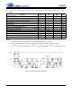
Figure 6. Typical Connection Diagram using the PLL
CS42426