
Manual

42 DS603F2
CS42418
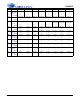
6. REGISTER DESCRIPTION
All registers are read/write except for the I.D. and Revision Register, OMCK/PLL_CLK Ratio Register, Clock Status
and Interrupt Status Register which are read only. See the following bit definition tables for bit assignment informa-
tion. The default state of each bit after a power-up sequence or reset is listed in each bit description.
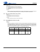
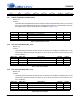
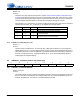
6.1 Memory Address Pointer (MAP)
Not a register
6.1.1 INCREMENT (INCR)
Default = 1
Function:
Memory Address Pointer auto increment control
0 - MAP is not incremented automatically.
1 - Internal MAP is automatically incremented after each read or write.
6.1.2 MEMORY ADDRESS POINTER (MAPX)
Default = 0000001
Function:
Memory Address Pointer (MAP). Sets the register address that will be read or written by the control
port.
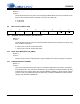
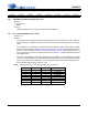
6.2 Chip I.D. and Revision Register (address 01h) (Read Only)
6.2.1 CHIP I.D. (CHIP_IDX)
Default = 1110
Function:
I.D. code for the CS42418. Permanently set to 1110.
6.2.2 CHIP REVISION (REV_IDX)
Default = xxxx
Function:
CS42418 revision level.
Revision C1 is coded as 0101
Revision C is coded as 0011.
76543210
INCR MAP6 MAP5 MAP4 MAP3 MAP2 MAP1 MAP0
76543210
Chip_ID3 Chip_ID2 Chip_ID1 CHIP_ID0 Rev_ID3 Rev_ID2 Rev_ID1 Rev_ID0