
User Manual


DS602F2 19
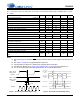
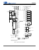
CS42416
VLS
VD
AOUTA1+
24
0.1 µF
+
10 µF
100 µF
0.1 µF
+
+
17
18
VQ
FILT+
36
37
0.1 µF
4.7 µF
VA
+
10 µF
0.1 µF
51
53
AOUTA1-
AOUTB1+
35
34
AOUTB1-
AOUTA2+
32
33
AOUTA2-
AOUTB2+
31
30
AOUTB2-
AOUTA3+
28
29
AOUTA3-
AOUTB3+
27
26
AOUTB3-
MUTEC
38
25
DGND
DGND
5
VLC
0.1 µF
6
3
60
59
1
64
61
2
63
8
7
SCL/CCLK
SDA/CDOUT
AD1/CDIN
RST
12
9
OMCK
ADC_LRCK
REFGND
19
AD0/CS
10
INT
11
55
RMCK
58
ADCIN1
57
ADCIN2
56
ADC_SDOUT
48
46
44
45
47
43
41
4
VAVD
0.1 µF
AGNDAGND
52 40
LPFLT
39
AINL+
AINL-
AINR+
AINR-
15
16
14
13
42
GPO1
GPO2
GPO3
GPO4
GPO5
GPO6
GPO7
DAC_SDIN1
ADC_SCLK
DAC_SDIN3
DAC_SDIN2
DAC_LRCK
DAC_SCLK
0.01 µF
0.1 µF
+
10 µF
+5 V
0.01 µF
0.01 µF
+3.3 V to +5 V
+
10 µF
0.1 µF 0.01 µF
Analog Output Buffer
2
and
Mute Circuit (optional)
Mute
Drive
(optional)
2700 pF*
2700 pF*
Left Analog Input
Right Analog Input
Analog
Input
Buffer
1
Analog
Input
Buffer
1
+VA
*
* Pull up or down as
required on startup if the
M ute C on trol is u sed.
*
Analog Output Buffer
2
and
Mute Circuit (optional)
Analog O utput Buffer
2
and
Mute Circuit (optional)
Analog Output Buffer
2
and
Mute Circuit (optional)
Analog Output Buffer
2
and
Mute Circuit (optional)
Analog Output Buffer
2
and
Mute Circuit (optional)
Connect DGND and AGND at single point near Codec
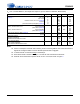
CFILT
3
RFILT
3
CRIP
3
2 k 2 k
** **
** Resistors are required for
I
2
C control port operation
1. S ee the A DC Input Filter section in the A ppendix.
2. S ee the D AC O utput Filter section in th e A ppendix.
3. See the PLL Filter section in the Appendix.
+1.8 V
to +5.0 V
DVD
Processor
27 MHz
Figure 6. Typical Connection Diagram using the PLL
CS42416