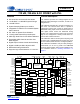
CS42416 110 dB, 192-kHz 6-Ch CODEC with PLL Features General Description Six 24-bit D/A, two 24-bit A/D Converters The CS42416 provides two analog-to-digital and six digital-to-analog delta-sigma converters, as well as an integrated PLL. 110 dB DAC / 114 dB ADC Dynamic Range -100 dB THD+N The CS42416 integrated PLL provides a low-jitter system clock. The internal stereo ADC is capable of independent channel gain control for single-ended or differential analog inputs.
CS42416 TABLE OF CONTENTS 1. CHARACTERISTICS AND SPECIFICATIONS ...................................................................................... 6 SPECIFIED OPERATING CONDITIONS ............................................................................................... 6 ABSOLUTE MAXIMUM RATINGS ......................................................................................................... 6 ANALOG INPUT CHARACTERISTICS ....................................................................
CS42416 6.7 Clock Control (address 06h) ........................................................................................................... 48 6.8 OMCK/PLL_CLK Ratio (address 07h) (Read Only) ....................................................................... 49 6.9 Clock Status (address 08h) (Read Only) ........................................................................................ 50 6.10 Volume Transition Control (address 0Dh) .........................................................
CS42416 Figure 17. OLM Configuration #1 .............................................................................................................. 31 Figure 18. OLM Configuration #2 .............................................................................................................. 32 Figure 19. OLM Configuration #3 .............................................................................................................. 33 Figure 20. OLM Configuration #4 ..................................
CS42416 LIST OF TABLES Table 1. Common OMCK Clock Frequencies ............................................................................................ 24 Table 2. Common PLL Output Clock Frequencies..................................................................................... 24 Table 3. Slave Mode Clock Ratios ............................................................................................................. 25 Table 4. Serial Audio Port Channel Allocations ............................
CS42416 1. CHARACTERISTICS AND SPECIFICATIONS (All Min/Max characteristics and specifications are guaranteed over the Specified Operating Conditions. Typical performance characteristics and specifications are derived from measurements taken at nominal supply voltages and TA = 25° C.) SPECIFIED OPERATING CONDITIONS (AGND=DGND=0, all voltages with respect to ground; OMCK=12.
CS42416 ANALOG INPUT CHARACTERISTICS (TA = 25° C; VA = 5 V, VD = 3.3 V, Logic “0” = DGND =AGND = 0 V; Logic “1” = VLS = VLC = 5 V; Measurement Bandwidth is 10 Hz to 20 kHz unless otherwise specified. Full-scale input sine wave, 997 Hz.; PDN_PLL = 1; OMCK = 12.288 MHz; Single-Speed Mode DAC_SCLK = 3.072 MHz; Double-Speed Mode DAC_SCLK = 6.144 MHz; Quad-Speed Mode DAC_SCLK = 12.288 MHz.
CS42416 A/D DIGITAL FILTER CHARACTERISTICS Parameter Symbol Min Typ Max Unit (Note 5) 0 - 0.47 Fs - - 0.035 dB (Note 5) 0.58 - - Fs Single-Speed Mode (2 to 50 kHz sample rates) Passband (-0.1 dB) Passband Ripple Stopband Stopband Attenuation -95 - - dB tgd - 12/Fs - s tgd - - 0.0 s (Note 5) 0 - 0.45 Fs - - 0.035 dB (Note 5) 0.68 - - Fs Total Group Delay (Fs = Output Sample Rate) Group Delay Variation vs.
CS42416 ANALOG OUTPUT CHARACTERISTICS (TA = 25° C; VA = 5 V, VD = 3.3 V, Logic “0” = DGND =AGND = 0 V; Logic “1” = VLS = VLC = 5V; Measurement Bandwidth 10 Hz to 20 kHz unless otherwise specified.; Full-scale output 997 Hz sine wave, Test load RL = 3 k, CL = 30 pF; PDN_PLL = 1; OMCK = 12.288 MHz; Single-Speed Mode, DAC_SCLK = 3.072 MHz; Double-Speed Mode, DAC_SCLK = 6.144 MHz; Quad-Speed Mode, DAC_SCLK = 12.288 MHz.
CS42416 D/A DIGITAL FILTER CHARACTERISTICS Fast Roll-Off Slow Roll-Off Parameter Min Typ Max Min Typ Max Combined Digital and On-chip Analog Filter Response - Single-Speed Mode - 48 kHz Passband (Note 9) to -0.01 dB corner 0 to -3 dB corner 0 Frequency Response 10 Hz to 20 kHz -0.01 StopBand 0.5465 StopBand Attenuation (Note 10) 90 Group Delay Passband Group Delay Deviation 0 - 20 kHz De-emphasis Error (Note 11) Fs = 32 kHz (Relative to 1 kHz) Fs = 44.1 kHz Fs = 48 kHz - 12/Fs - 0.4535 0.4998 +0.01 ±0.
CS42416 SWITCHING CHARACTERISTICS (TA = -10 to +70° C; VA = 5 V, VD =VLC= 3.3 V, VLS = 1.8 V to 5.25 V; Inputs: Logic 0 = DGND, Logic 1 = VLS, CL = 30 pF) Parameters Symbol RST Pin Low Pulse Width Min Typ Max Units 1 - - ms 30 - 200 kHz - 200 - ps RMS (Note 12) PLL Clock Recovery Sample Rate Range RMCK Output Jitter (Note 14) RMCK Output Duty Cycle (Note 15) 45 50 55 % OMCK Frequency (Note 13) 1.024 - 25.
CS42416 SWITCHING CHARACTERISTICS - CONTROL PORT - I²C™ FORMAT (TA = -10 to +70° C; VA = 5 V, VD =VLS= 3.3 V; VLC = 1.8 V to 5.25 V; Inputs: Logic 0 = DGND, Logic 1 = VLC, CL = 30 pF) Parameter Symbol Min Max Unit SCL Clock Frequency fscl - 100 kHz RST Rising Edge to Start tirs 500 - ns Bus Free Time Between Transmissions tbuf 4.7 - µs Start Condition Hold Time (prior to first clock pulse) thdst 4.0 - µs Clock Low time tlow 4.7 - µs Clock High Time thigh 4.0 - µs tsust 4.
CS42416 SWITCHING CHARACTERISTICS - CONTROL PORT - SPI™ FORMAT (TA = -10 to +70° C; VA = 5 V, VD =VLS= 3.3 V; VLC = 1.8 V to 5.25 V; Inputs: Logic 0 = DGND, Logic 1 = VLC, CL = 30 pF) Parameter Symbol Min Typ Max Units CCLK Clock Frequency fsck 0 - 6.0 MHz CS High Time Between Transmissions tcsh 1.
CS42416 DC ELECTRICAL CHARACTERISTICS (TA = 25° C; AGND=DGND=0, all voltages with respect to ground; OMCK=12.288 MHz; Master Mode) Parameter Symbol Min Typ Max Units IA ID ID ILC ILS Ipd - 75 85 51 250 13 250 - mA mA mA A mA A - 587 1.25 866 1.25 650 960 - mW mW mW mW - 60 40 - dB dB VQ Nominal Voltage VQ Output Impedance VQ Maximum allowable DC current - 2.7 50 0.01 - V k mA FILT+ Nominal Voltage FILT+ Output Impedance FILT+ Maximum allowable DC current - 5.0 35 0.
CS42416 DIGITAL INTERFACE CHARACTERISTICS (TA = +25° C) Parameters (Note 26) High-Level Input Voltage Low-Level Input Voltage High-Level Output Voltage at Io=2 mA Low-Level Output Voltage at Io=2 mA Serial Port, Control Port, MUTEC, GPOx High-Level Output Voltage at Io=100 A Low-Level Output Voltage at Io=100 A Input Leakage Current Input Capacitance MUTEC Drive Current Serial Port Control Port Serial Port Control Port (Note 27)Serial Port Control Port MUTEC, GPOx (Note 27) (Note 27)Serial Port Control
CS42416 NC NC VD DGND VLS RMCK NC ADCIN2 ADC_SDOUT ADCIN1 ADC_LRCK OMCK TEST ADC_SCLK DAC_SDIN2 DAC_SDIN3 2.
CS42416 RST 12 AINRAINR+ 13 14 Reset (Input) - The device enters a low power mode and all internal registers are reset to their default settings when low. Differential Right Channel Analog Input (Input) - Signals are presented differentially to the delta-sigma modulators via the AINR+/- pins. AINL+ AINL- 15 16 Differential Left Channel Analog Input (Input) - Signals are presented differentially to the delta-sigma modulators via the AINL+/- pins.
CS42416 3. TYPICAL CONNECTION DIAGRAMS +3.3 V to +5 V 10 µF 10 µF + 0.1 µF 0.01 µF 0.01 µF 0.1 µF + + 0.1 µF 0.01 µF 0.01 µF 0.1 µF + 51 4 VD VD 41 VA AOUTA1+ +3.3 V to +5.0 V CS8416 Receiver 48 47 S/PDIF 46 RMCK 45 44 43 42 53 0.
CS42416 + 3 .3 V to + 5 V 10 µF 10 µF + 0 .1 µ F 0 .0 1 µ F 0 .0 1 µ F 0 .1 µ F + + 0 .1 µ F 0 .0 1 µ F 0 .0 1 µ F 0 .1 µ F + 51 4 VD 41 VD VA 47 VA 46 45 44 43 42 + 1 .8 V to + 5 .0 V 53 0 .
CS42416 4. APPLICATIONS 4.1 Overview The CS42416 is a highly integrated mixed-signal 24-bit audio codec comprised of 2 analog-to-digital converters (ADC), implemented using multi-bit delta-sigma techniques, and 6 digital-to-analog converters (DAC). Other functions integrated within the codec include independent digital volume controls for each DAC, digital de-emphasis filters for DAC, digital gain control for ADC channels, ADC high-pass filters, and an on-chip voltage reference.
CS42416 4.2.2 High-Pass Filter and DC Offset Calibration The high-pass filter continuously subtracts a measure of the DC offset from the output of the decimation filter. The high-pass filter can be independently enabled and disabled. If the HPF_Freeze bit is set during normal operation, the current value of the DC offset for the corresponding channel is frozen and this DC offset will continue to be subtracted from the conversion result.
CS42416 4.3.3 Digital Volume and Mute Control Each DAC’s output level is controlled via the Volume Control registers operating over the range of 0 to -127 dB attenuation with 0.5 dB resolution. See “Volume Control (addresses 0Fh, 10h, 11h, 12h, 13h, 14h)” on page 53. Volume control changes are programmable to ramp in increments of 0.125 dB at the rate controlled by the SZC[1:0] bits in the Digital Volume Control register. See “Volume Transition Control (address 0Dh)” on page 51.
CS42416 4.4 Clock Generation The clock generation for the CS42416 is shown in the figure below. The internal MCLK is derived from the output of the PLL or a master clock source attached to OMCK. The mux selection is controlled by the SW_CTRLx bits and can be configured to manual switch mode only, or automatically switch on loss of PLL lock to the other source input. RMCK_DIVx bits 00 Internal MCLK ADC_LRCK (slave mode) PLL (256Fs) 8.192 49.
CS42416 4.4.2 OMCK System Clock Mode A special clock-switching mode is available that allows the clock that is input through the OMCK pin to be used as the internal master clock. This feature is controlled by the SW_CTRLx bits in register “Clock Control (address 06h)” on page 48. An advanced auto-switching mode is also implemented to maintain master clock functionality.
CS42416 When the device is clocked from OMCK, the frequency of OMCK must be at least twice the frequency of the fastest Slave Mode, SCLK. For example, if both serial ports are in Slave Mode with one SCLK running at 32x Fs and the other at 64x Fs, the slowest OMCK signal that can be used to clock the device is 128x Fs. When either serial port is in Slave Mode, its respective LRCK signal must be present for proper device operation. In Slave Mode, One-Line Mode #1 is supported; One-Line Mode #2 is not.
CS42416 Serial Inputs / Outputs left channel DAC #1 right channel DAC #2 One-Line Mode DAC channels 1,2,3,4,5,6 DAC_SDIN2 left channel DAC #3 right channel DAC #4 One-Line Mode not used DAC_SDIN3 left channel DAC #5 right channel DAC #6 One-Line Mode not used ADC_SDOUT left channel ADC #1 right channel ADC #2 One-Line Mode ADC channels 1,2,3,4,5,6 ADCIN1 left channel External ADC #3 right channel External ADC #4 ADCIN2 left channel External ADC #5 right channel External ADC #6 DAC_SDIN1 Table 4.
CS42416 4.5.2 Serial Audio Interface Formats The DAC_SP and ADC_SP digital audio serial ports support five formats with varying bit depths from 16 to 24 as shown in Figures 11 to 15. These formats are selected using the configuration bits in the registers, “Functional Mode (address 03h)” on page 43 and “Interface Formats (address 04h)” on page 45. For the diagrams below, Single-Speed Mode is equivalent to Fs = 32, 44.1, 48 kHz; Double-Speed Mode is for Fs = 64, 88.
CS42416 DAC_LRCK ADC_LRCK Left C ha nnel Rig ht C ha nnel DAC_SCLK ADC_SCLK DAC_SDINx ADC_SDOUT MSB +5 +4 +3 +2 +1 -1 -2 -3 -4 -5 LSB M SB -1 -2 -3 -4 +5 +4 +3 +2 +1 LSB I²S Mode, Data Valid on Rising Edge of SCLK Bits/Sample SCLK Rate(s) Master 16 18 to 24 Notes Slave 64 Fs 48, 64, 128 Fs Single-Speed Mode 64 Fs 64 Fs Double-Speed Mode 64 Fs 64 Fs Quad-Speed Mode 64, 128, 256 Fs 48, 64, 128 Fs Single-Speed Mode 64 Fs 64 Fs Double-Speed Mode 64 Fs 64 Fs Quad-Speed Mode Fig
CS42416 DAC_LRCK ADC_LRCK DAC_SCLK ADC_SCLK DAC_SDIN1 M SB ADC_SDOUT 64 clks 64 clks Left Channel Right C hannel LS B M SB LS B M SB LS B M SB LS B M SB LSB M SB D AC 1 DAC3 D AC5 DAC2 D AC4 20 clks 20 clks 20 clks 20 clks 20 clks A DC1 A DC3 A DC5 A DC2 A DC4 A DC6 20 clks 20 clks 20 clks 20 clks 20 clks 20 clks LS B M SB LSB MSB D AC6 20 clks One Line Data Mode #1, Data Valid on Rising Edge of SCLK Bits/Sample SCLK Rate(s) Notes Master 20 Slave 128 Fs 128 Fs
CS42416 4.5.3 ADCIN1/ADCIN2 Serial Data Format The two serial data lines which interface to the optional external ADCs, ADCIN1 and ADCIN2, support only left-justified, 24-bit samples at 64Fs or 128Fs. This interface is not affected by any of the serial port configuration register bit settings. These serial data lines are used when supporting One-Line Mode of operation with external ADCs attached. If these signals are not being used, they should be tied together and wired to GND via a pull-down resistor.
CS42416 4.5.4 One-Line Mode (OLM) Configurations 4.5.4.1 OLM Config #1 One-Line Mode Configuration #1 can support up to 6 channels of DAC data, and 6 channels of ADC data. This is the only configuration which will support up to 24-bit samples at a sampling frequency of 48 kHz on all channels for both the DAC and ADC.
CS42416 4.5.4.2 OLM Config #2 This configuration will support up to 6 channels of DAC data or 6 channels of ADC data and will handle up to 20-bit samples at a sampling-frequency of 96 kHz on all channels for both the DAC and ADC. The output data stream of the internal and external ADCs is configured to use the ADC_SDOUT output and run at the DAC Serial Port sample frequency.
CS42416 4.5.4.3 OLM Config #3 This configuration will support up to 6 channels of DAC data and 6 channels of ADC data. OLM Config #3 will handle up to 20-bit ADC samples at an Fs of 48 kHz and 24-bit DAC samples at an Fs of 48 kHz. Since the ADC’s data stream is configured to use the ADC_SDOUT output and the internal and external ADCs are clocked from the ADC_SP, the sample rate for the DAC Serial Port can be different from the sample rate of the ADC serial port.
CS42416 4.5.4.4 OLM Config #4 This One-Line Mode configuration can support up to 6 channels of DAC data on 2 DAC_SDIN pins and 2 channels of ADC data and will handle up to 24-bit samples at a sampling frequency of 48 kHz on all channels for both the DAC and ADC. The output data stream of the internal ADCs can be configured to run at the DAC_SP clock speeds or to run at the ADC_SP rate. The DAC_SP and ADC_SP can operate at different Fs rates.
CS42416 M CLK 64Fs,128Fs ADC_SCLK RMCK SCLK_PORT1 LRCK_PORT1 ADC_LRCK SDIN_PORT1 ADC_SDOUT ADCIN1 ADCIN2 SDIN_PORT2 64Fs,128Fs, 256Fs DAC_SCLK SCLK_PORT2 DAC_LRCK DAC_SDIN1 DAC_SDIN2 LRCK_PORT2 DAC_SDIN3 SDOUT3_PORT2 CS42416 SDOUT1_PORT2 SDOUT2_PORT2 DIGITAL AUDIO PROCESSOR Figure 20. OLM Configuration #4 4.6 Control Port Description and Timing The control port is used to access the registers, allowing the CS42416 to be configured for the desired operational modes and formats.
CS42416 4.6.2 I²C Mode In I²C mode, SDA is a bidirectional data line. Data is clocked into and out of the part by the clock, SCL. There is no CS pin. Pins AD0 and AD1 form the two least-significant bits of the chip address and should be connected through a resistor to VLC or DGND as desired. The state of the pins is sensed while the CS42416 is being reset. The signal timings for a read and write cycle are shown in Figure 22 and Figure 23.
CS42416 0 1 2 3 4 5 6 7 8 9 10 11 12 13 14 15 16 17 18 19 20 21 22 23 24 25 26 27 28 SCL CHIP ADDRESS (WRITE) SDA 1 0 0 1 STOP MAP BYTE 1 AD1 AD0 0 INCR 6 5 4 3 ACK START 2 1 CHIP ADDRESS (READ) 1 0 0 0 1 DATA 1 AD1 AD0 1 ACK START 7 ACK DATA +1 0 7 ACK 0 DATA + n 7 0 NO ACK STOP Figure 23. Control Port Timing, I²C Read Since the read operation cannot set the MAP, an aborted write operation is used as a preamble.
CS42416 4.8 Reset and Power-Up Reliable power-up can be accomplished by keeping the device in reset until the power supplies, clocks and configuration pins are stable. It is also recommended that reset be activated if the analog or digital supplies drop below the recommended operating condition to prevent power-glitch-related issues. When RST is low, the CS42416 enters a low-power mode and all internal states are reset, including the control port and registers, and the outputs are muted.
CS42416 5.
CS42416 Addr Function 13h 14h 15h 16h 17h 18h 19h 1Ah 1Bh 1Ch 1Dh 1Eh 1Fh 20h 21h 22h 40 Vol. Control A3 page 53 default Vol. Control B3 page 53 default Reserved page 53 default Reserved page 53 default Channel Invert page 53 default Mixing Ctrl Pair 1 page 53 default Mixing Ctrl Pair 2 page 53 default Mixing Ctrl Pair 3 page 53 default Reserved page 53 default ADC Left Ch. Gain page 55 default ADC Right Ch.
CS42416 Addr Function 23h 24h27h Interrupt Mode LSB page 57 default Reserved default 28h 29h 2Ah 2Bh 2Ch 2Dh 2Eh 2Fh MUTEC page 57 default GPO7 page 58 default GPO6 page 58 default GPO5 page 58 default GPO4 page 58 default GPO3 page 58 default GPO2 page 58 default GPO1 page 58 default DS602F2 7 6 5 4 3 2 1 0 UNLOCK0 Reserved Reserved Reserved Reserved Reserved OF0 Reserved 0 0 0 0 0 0 0 0 Reserved Reserved Reserved Reserved Reserved Reserved Reserved Reserved 0
CS42416 6. REGISTER DESCRIPTION All registers are read/write except for the I.D. and Revision Register, OMCK/PLL_CLK Ratio Register, Clock Status and Interrupt Status Register which are read only. See the following bit definition tables for bit assignment information. The default state of each bit after a power-up sequence or reset is listed in each bit description. 6.1 Memory Address Pointer (MAP) Not a register 7 INCR 6.1.
CS42416 6.3 Power Control (address 02h) 7 Reserved 6.3.1 6 PDN_PLL 5 PDN_ADC 4 Reserved 3 PDN_DAC3 2 PDN_DAC2 1 PDN_DAC1 0 PDN POWER DOWN PLL (PDN_PLL) Default = 0 Function: When enabled, the PLL is held in a reset state. It is advised that any change of this bit be made while the DACs are muted or the power-down bit (PDN) is enabled to eliminate the possibility of audible artifacts. 6.3.
CS42416 6.4.2 ADC FUNCTIONAL MODE (ADC_FMX) Default = 00 00 - Single-Speed Mode (4 to 50 kHz sample rates) 01 - Double-Speed Mode (50 to 100 kHz sample rates) 10 - Quad-Speed Mode (100 to 192 kHz sample rates) 11 - Reserved Function: Selects the required range of sample rates for the ADC serial port (ADC_SP). These bits must be set to the corresponding sample rate range when the ADC_SP is in Master or Slave Mode. 6.4.
CS42416 6.5 Interface Formats (address 04h) 7 DIF1 6.5.1 6 DIF0 5 ADC_OL1 4 ADC_OL0 3 DAC_OL1 2 DAC_OL0 1 Reserved 0 CODEC_RJ16 DIGITAL INTERFACE FORMAT (DIFX) Default = 01 Function: These bits select the digital interface format used for the ADC & DAC Serial Port when not in One-Line Mode. The required relationship between the Left/Right clock, serial clock, and serial data is defined by the Digital Interface Format and the options are detailed in Figures 11-13.
CS42416 6.5.4 CODEC RIGHT-JUSTIFIED BITS (CODEC_RJ16) Default = 0 Function: This bit determines how many bits to use during Right-Justified Mode for the DAC and ADC. By default, the DAC and ADC will be in RJ24 bits, but can be set to RJ16 bits. 0 - 24 bit mode. 1 - 16 bit mode. 6.6 Misc Control (address 05h) 7 Ext ADC SCLK 6.6.
CS42416 6.6.4 INTERPOLATION FILTER SELECT (FILT_SEL) Default = 0 Function: This feature allows the user to select whether the DAC interpolation filter has a fast- or slow roll-off. For filter characteristics, please See “D/A Digital Filter Characteristics” on page 10. 0 - Fast roll-off. 1 - Slow roll-off. 6.6.5 HIGH-PASS FILTER FREEZE (HPF_FREEZE) Default = 0 Function: When this bit is set, the internal high-pass filter for the selected channel will be disabled.
CS42416 6.7 Clock Control (address 06h) 7 RMCK_DIV1 6.7.1 6 RMCK_DIV0 5 OMCK Freq1 4 OMCK Freq0 3 PLL_LRCK 2 SW_CTRL1 1 SW_CTRL0 0 FRC_PLL_LK RMCK DIVIDE (RMCK_DIVX) Default = 00 Function: Divides/multiplies the internal MCLK, either from the PLL or OMCK, by the selected factor. RMCK_DIV1 RMCK_DIV0 0 0 1 1 0 1 0 1 Description Divide by 1 Divide by 2 Divide by 4 Multiply by 2 Table 9. RMCK Divider Settings 6.7.
CS42416 6.7.4 MASTER CLOCK SOURCE SELECT (SW_CTRLX) Default = 00 Function: These two bits, along with the UNLOCK bit in register “Interrupt Status (address 20h) (Read Only)” on page 56, determine the master clock source for the CS42416. When SW_CTRL1 and SW_CTRL0 are set to '00'b, selecting the output of the PLL as the internal clock source, and the PLL becomes unlocked, RMCK will equal OMCK, but all internal and serial port timings are not valid.
CS42416 6.9 Clock Status (address 08h) (Read Only) 7 Reserved 6.9.1 6 Reserved 5 Reserved 4 Reserved 3 Active_CLK 2 PLL_CLK2 1 PLL_CLK1 0 PLL_CLK0 SYSTEM CLOCK SELECTION (ACTIVE_CLK) Default = x 0 - Output of PLL 1 - OMCK Function: This bit identifies the source of the internal system clock (MCLK). 6.9.2 PLL CLOCK FREQUENCY (PLL_CLKX) Default = xxx Function: The CS42416 detects the ratio between the OMCK and the recovered clock from the PLL.
CS42416 6.10 Volume Transition Control (address 0Dh) 7 Reserved 6 SNGVOL 5 SZC1 4 SZC0 3 AMUTE 2 MUTE ADC_SP 1 RAMP_UP 0 RAMP_DN 6.10.1 SINGLE VOLUME CONTROL (SNGVOL) Default = 0 Function: The individual channel volume levels are independently controlled by their respective Volume Control registers when this function is disabled. When enabled, the volume on all channels is determined by the A1 Channel Volume Control register and the other Volume Control registers are ignored. 6.10.
CS42416 6.10.3 AUTO-MUTE (AMUTE) Default = 1 0 - Disabled 1 - Enabled Function: The digital-to-analog converters of the CS42416 will mute the output following the reception of 8192 consecutive audio samples of static 0 or -1. A single sample of non-static data will release the mute. Detection and muting is done independently for each channel. The quiescent voltage on the output will be retained, and the MUTEC pin will go active during the mute period.
CS42416 6.12 Volume Control (addresses 0Fh, 10h, 11h, 12h, 13h, 14h) 7 xx_VOL7 6 xx_VOL6 5 xx_VOL5 4 xx_VOL4 3 xx_VOL3 2 xx_VOL2 1 xx_VOL1 0 xx_VOL0 6.12.1 VOLUME CONTROL (XX_VOL) Default = 0 Function: The Digital Volume Control registers allow independent control of the signal levels in 0.5 dB increments from 0 to -127 dB. Volume settings are decoded as shown in Table 13. The volume changes are implemented as dictated by the Soft and Zero Cross bits (SZC[1:0]).
CS42416 6.14.2 ATAPI CHANNEL-MIXING AND MUTING (PX_ATAPIX) Default = 01001 Function: The CS42416 implements the channel-mixing functions of the ATAPI CD-ROM specification. The ATAPI functions are applied per A-B pair. Refer to Table 14 and Figure 9 for additional information.
CS42416 6.15 ADC Left Channel Gain (address 1Ch) 7 Reserved 6 Reserved 5 LGAIN5 4 LGAIN4 3 LGAIN3 2 LGAIN2 1 LGAIN1 0 LGAIN0 6.15.1 ADC LEFT CHANNEL GAIN (LGAINX) Default = 00h Function: The level of the left analog channel can be adjusted in 1 dB increments as dictated by the Soft and Zero Cross bits (SZC[1:0]) from +15 to -15 dB. Levels are decoded in two’s complement, as shown in Table 15. 6.
CS42416 6.17.2 DE-EMPHASIS SELECT BITS (DE-EMPHX) Default = 00 00 - Reserved 01 - De-Emphasis for 32 kHz sample rate. 10 - De-Emphasis for 44.1 kHz sample rate. 11 - De-Emphasis for 48 kHz sample rate. Function: Used to specify which de-emphasis filter to apply when the “Force PLL Lock (FRC_PLL_LK)” on page 49 is enabled. 6.17.
CS42416 6.19 Interrupt Mask (address 21h) 7 UNLOCKM 6 Reserved 5 Reserved 4 Reserved 3 Reserved 2 Reserved 1 OverFlowM 0 Reserved Default = 00000000 Function: The bits of this register serve as a mask for the interrupt sources found in the register “Interrupt Status (address 20h) (Read Only)” on page 56. If a mask bit is set to 1, the error is unmasked, meaning that its occurrence will affect the INT pin and the status register.
CS42416 6.21.2 CHANNEL MUTES SELECT (M_AOUTXX) Default = 1111 0 - Channel mute is not mapped to the MUTEC pin 1 - Channel mute is mapped to the MUTEC pin Function: Determines which channel mutes will be mapped to the MUTEC pin. If no channel mute bits are mapped, then the MUTEC pin is driven to the “active” state as defined by the POLARITY bit. These Channel Mute Select bits are “ANDed” together in order for the MUTEC pin to go active.
CS42416 6.22.3 FUNCTIONAL CONTROL (FUNCTIONX) Default = 00000 Function: Mute Mode - If the pin is configured as a dedicated mute pin, the functional bits determine which channel mutes will be mapped to this pin according to the following table.
CS42416 7. PARAMETER DEFINITIONS Dynamic Range The ratio of the rms value of the signal to the rms sum of all other spectral components over the specified bandwidth. Dynamic Range is a signal-to-noise ratio measurement over the specified band width made with a -60 dBFS signal. 60 dB is added to resulting measurement to refer the measurement to full-scale. This technique ensures that the distortion components are below the noise level and do not effect the measurement.
CS42416 8. APPENDIX A: EXTERNAL FILTERS 8.1 ADC Input Filter The analog modulator samples the input at 6.144 MHz (internal MCLK=12.288 MHz). The digital filter will reject signals within the stopband of the filter. However, there is no rejection for input signals which are (n 6.144 MHz) the digital passband frequency, where n=0,1,2,... Refer to Figure 24 for a recommended analog input buffer that will attenuate any noise energy at 6.
CS42416 9. APPENDIX B: PLL FILTER 9.1 9.1.1 External Filter Components General The PLL behavior is affected by the external filter component values in the Typical Connection Diagrams. Figure 5 and Figure 6 show the recommended configuration of the two capacitors and one resistor that comprise the PLL filter. The external PLL component values listed in Table 16 have a high corner-frequency jitter-attenuation curve, take a short time to lock, and offer good output jitter performance.
CS42416 9.1.3 Circuit Board Layout RFILT CRIP VA AGND LPFLT Board layout and capacitor choice affect each other and determine the performance of the PLL. Figure 26 illustrates a suggested layout for the PLL filter components and for bypassing the analog supply voltage. The 10 µF bypass capacitor is an electrolytic in a surface-mount case A or thru-hole package. RFILT, CFILT, CRIP, and the 0.1 µF decoupling capacitor are in an 0805 form factor. The 0.
CS42416 0 0 -10 -10 -20 -20 -30 -30 -40 -40 -50 -50 Amplitude (dB) Amplitude (dB) 10.APPENDIX C: ADC FILTER PLOTS -60 -70 -80 -60 -70 -80 -90 -90 -100 -100 -110 -110 -120 -120 -130 -130 -140 0.0 0.1 0.2 0.3 0.4 0.5 0.6 0.7 0.8 0.9 -140 0.40 1.0 Frequency (normalized to Fs) 0.42 0.44 0.46 0.48 0.50 0.52 0.54 0.56 0.58 0.60 Frequency (normalized to Fs) Figure 27. Single-Speed Mode Stopband Rejection Figure 28. Single-Speed Mode Transition Band 0.
CS42416 0.10 0 -1 0.08 -2 0.05 -3 0.03 Amplitude (dB) Amplitude (dB) -4 -5 -6 0.00 -0.03 -7 -0.05 -8 -0.08 -9 -10 0.40 0.43 0.45 0.48 0.50 0.53 -0.10 0.00 0.55 Frequency (normalized to Fs) 0.10 0.20 0.25 0.30 0.35 0.40 0.45 0.50 Figure 34. Double-Speed Mode Passband Ripple 0 0 -10 -10 -20 -20 -30 -30 -40 -40 Amplitude (dB) -50 -60 -70 -80 -50 -60 -70 -80 -90 -90 -100 -100 -110 -110 -120 -130 -120 0.0 0.1 0.2 0.3 0.4 0.5 0.6 0.7 0.8 0.9 0.2 1.0 0.
CS42416 11.APPENDIX D: DAC FILTER PLOTS 0 20 20 40 40 Amplitude (dB) Amplitude (dB) 0 60 60 80 80 100 100 120 120 0.4 0.5 0.6 0.7 0.8 Frequency(normalized to Fs) 0.9 1 Figure 39. Single-Speed (fast) Stopband Rejection 0.4 0.42 0.44 0.46 0.48 0.5 0.52 Frequency(normalized to Fs) 0.54 0.56 0.58 0.6 Figure 40. Single-Speed (fast) Transition Band 0.02 0 1 0.015 2 0.01 0.005 4 Amplitude (dB) Amplitude (dB) 3 5 6 0 0.005 7 0.01 8 0.015 9 10 0.45 0.46 0.47 0.
CS42416 0.02 0 1 0.015 2 0.01 3 Amplitude (dB) Amplitude (dB) 0.005 4 5 6 0 0.005 7 0.01 8 0.015 9 10 0.45 0.02 0.46 0.47 0.48 0.49 0.5 0.51 Frequency(normalized to Fs) 0.52 0.53 0.54 0.55 Figure 45. Single-Speed (slow) Transition Band (detail) 0.1 0.15 0.2 0.25 0.3 Frequency(normalized to Fs) 0.35 0.4 0.45 0.5 0 20 20 40 40 Amplitude (dB) Amplitude (dB) 0.05 Figure 46. Single-Speed (slow) Passband Ripple 0 60 60 80 80 100 100 120 0 120 0.4 0.5 0.6 0.
CS42416 0 20 20 40 40 Amplitude (dB) Amplitude (dB) 0 60 60 80 80 100 100 120 120 0.2 0.3 0.4 0.5 0.6 0.7 Frequency(normalized to Fs) 0.8 0.9 1 Figure 51. Double-Speed (slow) Stopband Rejection 0.2 0.3 0.4 0.5 0.6 Frequency(normalized to Fs) 0.7 0.8 Figure 52. Double-Speed (slow) Transition Band 0 0.02 1 0.015 2 0.01 0.005 4 Amplitude (dB) Amplitude (dB) 3 5 6 0 0.005 7 0.01 8 0.015 9 10 0.45 0.46 0.47 0.48 0.49 0.5 0.51 Frequency(normalized to Fs) 0.52 0.
CS42416 0.2 0 1 0.15 2 0.1 3 Amplitude (dB) Amplitude (dB) 0.05 4 5 6 0 0.05 7 0.1 8 0.15 9 10 0.45 0.2 0.46 0.47 0.48 0.49 0.5 0.51 Frequency(normalized to Fs) 0.52 0.53 0.54 0.55 Figure 57. Quad-Speed (fast) Transition Band (detail) 0 0.05 0.1 0.15 Frequency(normalized to Fs) 0.2 0.25 Figure 58. Quad-Speed (fast) Passband Ripple 0 0 20 40 40 Amplitude (dB) Amplitude (dB) 20 60 60 80 80 100 100 120 120 0.1 0.2 0.3 0.4 0.5 0.6 0.
CS42416 12.PACKAGE DIMENSIONS 64L LQFP PACKAGE DRAWING E E1 D D1 1 e B A A1 L DIM A A1 B D D1 E E1 e* L MIN --0.002 0.007 0.461 0.390 0.461 0.390 0.016 0.018 0.000° * Nominal pin pitch is 0.50 mm INCHES NOM 0.55 0.004 0.008 0.472 BSC 0.393 BSC 0.472 BSC 0.393 BSC 0.020 BSC 0.024 4° MAX 0.063 0.006 0.011 0.484 0.398 0.484 0.398 0.024 0.030 7.000° MILLIMETERS NOM 1.40 0.10 0.20 12.0 BSC 10.0 BSC 12.0 BSC 10.0 BSC 0.50 BSC 0.60 4° MIN --0.05 0.17 11.70 9.90 11.70 9.90 0.40 0.45 0.00° MAX 1.
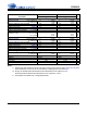
CS42416 13.ORDERING INFORMATION Product CS42416 Description Package 110 dB, 192 kHz 64-pin 6-Ch Codec LQFP with PLL CDB42428 CS42416 Evaluation Board Pb-Free Grade Temp Range Yes Commercial -10° to +70° C No - - Container Order # Tray CS42416-CQZ Tape & Reel CS42416-CQZR - CDB42428 14.REFERENCES 1) Cirrus Logic, Audio Quality Measurement Specification, Version 1.0, 1997. http://www.cirrus.com/products/papers/meas/meas.
CS42416 15.REVISION HISTORY Release Date Changes F1 November 2005 F2 March 2014 Final Release • Added Revision History table on page 71. • Updated registers 6.6.6 and 6.6.7 on page 47. • Updated registers 6.7.4 and 6.7.5 on page 49. • Updated PLL components in Table 16 on page 62. • Added OMCK Frequency specification in the Switching Characteristics table on page 11. • Updated ADC Input Impedance and Offset Error specifications in the Analog Input Characteristics table on page 7.